



 日本語
日本語
 한국어
한국어

What Is a PCB? Printed Circuit Board Explained
WHAT IS A PCB? A PCB (Printed Circuit Board) is a flat, non-conductive board designed to mechanically support electronic components and electrically connect them through etched copper pathways called traces. As the foundation of modern electronics, PCBs are used in almost every device, from simple consumer products like calculators to advanced systems in aerospace, automotive, and industrial applications.
If you have ever wondered what powers your smartphone, laptop, or even your car's dashboard, the answer almost always involves a printed circuit board. Understanding PCB meaning is essential for anyone working in electronics, engineering, or product development.
In this comprehensive guide, we break down what a circuit board is, how it works, what it's made of, the different types available, how they are manufactured, and how to choose the right one for your project. Whether you are a student, hobbyist, engineer, or procurement manager, this article covers everything you need to know about PCBs.
What Does PCB Stand For?
PCB stands for printed circuit board. The name has two parts worth understanding:
"Printed" refers to the manufacturing method. The copper wiring pattern is transferred onto the board photographically and chemically, similar in spirit to printing an image, rather than being wired by hand. This printing/etching process is what makes mass production of reliable, compact electronic circuits possible.
"Circuit board" describes the object itself: a rigid (or flexible) board whose purpose is to hold a complete electrical circuit.
You may also hear related terms:
PCBA: Printed Circuit Board Assembly — a fully populated board with all components soldered on
PWB: Printed Wiring Board — an older, less common term for the same thing
Further Reading: PCB vs PCBA: Key Differences in Manufacturing, Cost & Buying
KEY TAKEAWAYSPCB definition: PCB stands for Printed Circuit Board — a non-conductive board with etched copper pathways that create electrical connections.Core function: PCBs provide both mechanical support and electrical connectivity for electronic components.Main classifications: PCBs are classified by layer count (single-layer, double-layer, multilayer) and substrate type (rigid, flex, rigid-flex, metal-core, etc.).Manufacturing process: PCB manufacturing involves precision steps including imaging, etching, lamination, drilling, plating, and testing.Selection factors: Choosing the right PCB requires balancing circuit complexity, material properties, thermal requirements, production volume, and budget.
What Is a Circuit Board Made Of? Layer-by-Layer Anatomy
If you sliced a standard PCB down the middle, you would see a laminated sandwich. A typical rigid board is about 1.6 mm thick, and each layer in the stack has a specific job.
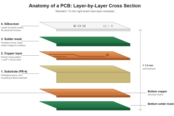
1. Substrate (the base). The structural core of the board, most commonly FR-4, a fiberglass-reinforced epoxy laminate. FR-4 is an insulator; it does not conduct electricity, and it is flame-retardant (that is what the "FR" means). Other substrates serve special needs: polyimide film for flexible circuits, aluminum cores for boards that must shed heat (such as LED lighting), and PTFE-based laminates for high-frequency RF designs.
2. Copper layer(s). A thin foil of copper bonded to the substrate, then chemically etched so that only the designed wiring pattern remains. Standard copper thickness is 1 oz per square foot, which works out to about 35 μm, roughly half the width of a human hair. A board can have one copper layer, two (one per side), or many internal layers in a multilayer stackup.
3. Solder mask. The colored polymer coating over the copper. Its jobs are to insulate the traces, prevent accidental solder bridges during assembly, and protect copper from oxidation. Green is traditional, but the color is purely cosmetic; blue, red, black, white, and purple boards are electrically identical.
4. Silkscreen. The printed white (usually) lettering on top: component labels like R1, C3, and U2, polarity marks, logos, and version numbers. Silkscreen has no electrical function. It exists so humans can assemble, test, and repair the board.
The features built into those layers
Beyond the layers themselves, every circuit board uses a small vocabulary of copper features:
Traces: the thin copper lines that act as fixed wires, carrying signals and power between components.
Pads: exposed copper areas where component pins are soldered.
Vias: small plated holes that carry a signal from one copper layer to another. Through vias span the whole board; blind and buried vias connect only some layers in high-density designs.
Planes (pours): large continuous copper areas, typically used for ground or power. Planes lower resistance, stabilize voltage, and improve signal quality.
Annular ring: the ring of copper left around a drilled hole. Too little annular ring is one of the most common fabrication defects flagged in design review.
Surface finish: a coating (HASL, ENIG, or OSP are the common ones) applied to exposed pads so they stay solderable between fabrication and assembly.
How Does a PCB Work?
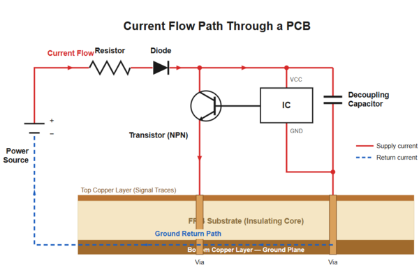
A printed circuit board works by giving electric current fixed, engineered paths to follow. Understanding this takes about four steps:
Step 1: Power enters the board. Current arrives from a battery, a USB port, or a power connector and flows onto a copper trace or power plane.
Step 2: Traces route current to components. Copper is an excellent conductor, and the FR-4 around it is an excellent insulator, so current stays confined to the designed path. Each trace is sized for its job: a hair-thin trace can carry a data signal, while a wide trace or plane carries motor or power currents. Trace width is a real engineering decision, because an undersized trace overheats exactly like an undersized wire.
Step 3: Components do the work. The board itself processes nothing. Resistors limit current, capacitors store and release charge, diodes force current one way, transistors switch and amplify, and integrated circuits perform logic. The PCB's contribution is to hold these parts in exact positions and connect pin A to pin B with near-zero error, every time, on every board produced.
Step 4: Current returns through ground. Every circuit is a loop. After passing through components, current returns via the ground plane or ground traces to the power source. In fast digital designs, the quality of this return path largely determines whether the board is quiet and reliable or plagued by noise.
One clarifying mental model: a schematic is the abstract drawing of a circuit, and the PCB is that drawing made physical. Layout, meaning where each part sits and how each trace runs, is not cosmetic. Two boards with identical schematics can behave very differently if one has poor layout, which is why PCB design is a distinct engineering discipline rather than a drawing exercise.
Further Reading: How to Convert Schematic to Gerber Files for PCB Manufacturing?
Why PCBs Replaced Wires: Advantages and Limitations
Before printed circuit boards, electronics were built with point-to-point wiring: every connection hand-soldered, wire by wire, between terminals. A 1950s television built this way contained a dense nest of wires, each one a potential mistake. Understanding what PCBs fixed explains why they are universal today.
Advantages of PCBs:
Miniaturization. Copper traces pack far more connections into far less space than physical wires. Smartphones are possible only because of high-density multilayer boards.
Repeatability. A PCB design is manufactured photographically, so board number 10,000 is electrically identical to board number 1. Hand wiring can never achieve this.
Reliability. Soldered joints on rigid pads resist vibration and fatigue far better than hanging wires. This is why automotive and aerospace electronics standardized on PCBs decades ago.
Lower cost at volume. Etching and automated assembly replace skilled manual labor, collapsing the per-unit cost of complex circuits.
Easier diagnosis. Silkscreen labels and fixed layouts mean a technician can find R17 on any copy of the board in seconds.
Limitations worth knowing:
Hard to modify after fabrication. Changing a circuit on a finished PCB means cutting traces and soldering jumper wires, acceptable for one prototype fix, not for production. Design errors are cheap on screen and expensive on copper.
Upfront design effort. A breadboard circuit can be rearranged in minutes; a PCB requires layout work and fabrication lead time before you hold anything.
Thermal and signal constraints. Dense boards concentrate heat, and high-speed signals demand careful routing. These are solvable problems, but they are the designer's responsibility.
This trade-off defines when each tool is used: breadboards for experiments, PCBs for anything that must be repeated, shipped, or trusted.
Further Reading: PCB vs Breadboard: Understanding Their Roles in Electronics Development
Types of PCBs: Which Board for Which Job
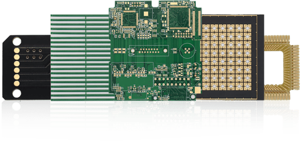
Printed circuit boards are classified two ways: by layer count and by mechanical construction. The table below covers the types you will actually encounter.
| PCB Type | Structure | Typical Applications | Relative Cost |
|---|---|---|---|
| Single-Layer | Copper layer on one side only | Calculators, LED strips, simple appliances, toys | Lowest |
| Double-Layer | Copper layers on both sides connected through vias | Power supplies, amplifiers, industrial controls, most hobby projects | Low |
| Multilayer (4–20+ layers) | Multiple internal copper layers laminated inside the PCB stackup | Smartphones, motherboards, network equipment, medical devices | Moderate to high |
| Rigid | Solid FR-4 core that maintains a fixed shape | Default construction for most electronic products | Baseline |
| Flexible (Flex) | Polyimide film substrate that can bend and fold | Cameras, wearables, printers, and applications requiring curved circuits | Higher |
| Rigid-flex | Rigid sections connected by flexible circuit areas | Foldable devices, aerospace systems, compact medical instruments | High |
| Metal-core (MCPCB) | Aluminum or copper core designed for improved heat dissipation | High-power LED lighting and power conversion systems | Moderate |
| High-frequency / RF | Low-dielectric-loss laminates such as Rogers or PTFE/Teflon for GHz-range signals | Radar systems, satellite communications, 5G infrastructure, microwave devices | High |
| Ceramic | Alumina, aluminum nitride, or beryllium oxide substrate with high thermal conductivity and temperature stability | High-power LEDs, power semiconductors, aerospace, military electronics | High |
| HDI | Microvias and ultra-fine traces designed for extreme circuit density | Flagship smartphones and high pin-count processor applications | High |
Two practical selection rules cut through the options. First, layer count follows circuit complexity: a hobby sensor board is comfortable on 2 layers, a design with a modern microcontroller and USB usually deserves 4 layers (the extra ground plane noticeably improves signal quality for a small cost premium), and dense digital systems climb from there. Second, construction follows the mechanical environment: if the board must bend, fit a curved enclosure, or dissipate serious heat, that requirement, not the circuit, picks the board type.
How Are PCBs Made? The Manufacturing Process in 13 Steps
Understanding how PCBs are made helps you appreciate the precision and complexity behind every board. The full fabrication process involves dozens of individual steps, but here are the core stages:
Step 1: Design and Gerber File Generation
Everything starts with a schematic and PCB layout created in ECAD software (Altium, KiCad, Eagle, OrCAD, etc.). The finished design is exported as Gerber files — the industry-standard format that describes each copper layer, solder mask, silkscreen, and drill pattern.
Tips: Before sending files to a manufacturer, run a DFM (Design for Manufacturing) check to catch issues that could cause fabrication failures or extra costs.
Step 2: Inner Layer Imaging and Etching
For multilayer boards, the process begins with the inner copper layers:
A photosensitive dry film is applied to the copper-clad substrate
The Gerber pattern is exposed onto the film using UV light (direct imaging or phototool)
Unexposed film is developed away, leaving the desired circuit pattern protected
The board is submerged in etchant (typically ferric chloride or ammonium persulfate) to dissolve unprotected copper
The remaining protective film is stripped, revealing the finished inner-layer copper pattern
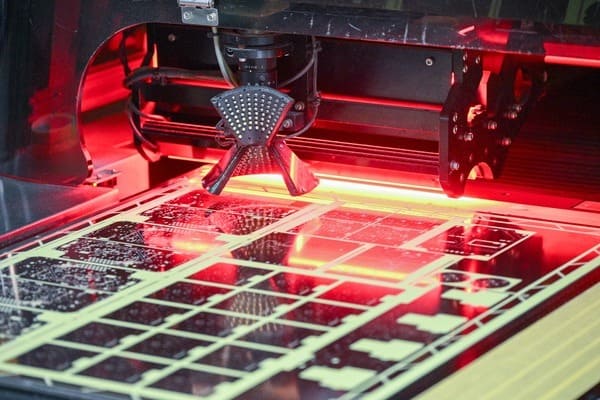
Step 3: Automated Optical Inspection (AOI)
Each inner layer is scanned by an AOI machine that compares the etched copper to the digital design file, detecting opens, shorts, and defects before layers are permanently laminated together.
Step 4: Layup and Lamination
All inner layers are stacked together with sheets of prepreg (partially cured epoxy-glass bonding material) between them, plus outer copper foils on the top and bottom. The entire stack is placed in a hydraulic press under high heat and pressure. The prepreg melts, flows, and fully cures, fusing all layers into a single solid board.
Step 5: Drilling
High-speed CNC drill machines create thousands of precision holes — for through-hole component leads, vias, mounting holes, and tooling holes. Drill diameters can be as small as 0.15 mm (0.006 in).
Step 6: Plating (Copper Deposition)
The drilled holes are chemically plated with copper through an electroplating process, creating a conductive barrel inside each via that electrically connects all layers.
Step 7: Outer Layer Imaging and Etching
The same imaging-and-etching process used for inner layers is repeated on the outer copper surfaces, creating the top and bottom trace patterns.
Step 8: Solder Mask Application
A liquid photoimageable solder mask is applied across the entire board surface, then exposed and developed so that only component pads and test points remain uncovered. The mask is then fully cured.
Step 9: Surface Finish
Exposed copper pads receive a protective surface finish to prevent oxidation and ensure good solderability. Common finishes:
HASL (Hot Air Solder Leveling) — traditional, low cost
ENIG (Electroless Nickel Immersion Gold) — flat, long shelf life, premium
OSP (Organic Solderability Preservative) — thin, low-cost, lead-free
Immersion Silver / Immersion Tin — mid-range options
Further Reading: HASL vs ENIG: Which PCB Surface Finish Should You Choose?
Step 10: Silkscreen Printing
Component labels, logos, and reference designators are printed onto the board surface using either screen printing or inkjet legend printing.
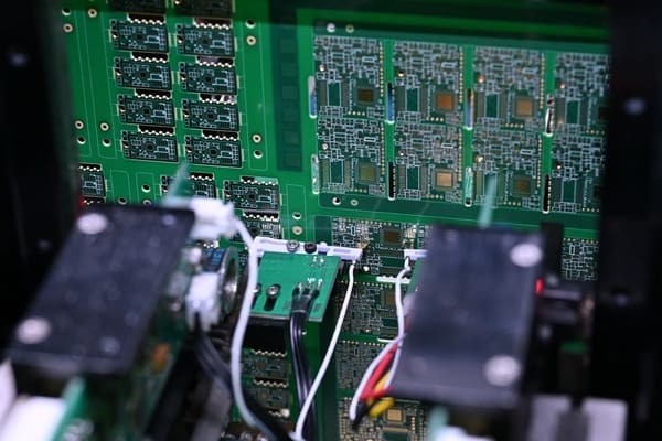
Step 11: Electrical Testing (E-Test / Flying Probe)
Every finished board undergoes electrical testing to verify there are no open circuits or short circuits. Flying probe testers use movable needle probes to contact test points across the board.
Step 12: Profiling / Routing / V-Scoring
Individual boards are separated from the larger manufacturing panel using CNC routing, V-scoring, or punch depaneling.
Step 13: Final Quality Inspection and Packaging
Boards receive a final visual inspection, are vacuum-sealed in ESD-safe packaging, and are shipped to the customer or sent on to assembly.
The PCB manufacturing process requires precise control at every stage, from verifying design files and producing inner layers to drilling, plating, surface finishing, and final inspection. Even a small issue during fabrication can affect board reliability, which makes choosing an experienced manufacturing partner critical.
A PCB manufacturer like PCBgogo provides end-to-end PCB and PCBA manufacturing support, helping engineers move from validated Gerber files to production-ready circuit boards. Its manufacturing capabilities cover rigid PCBs, flexible PCBs, and metal core PCBs, with surface finishing options such as HASL, ENIG, and OSP to meet different application requirements.
To ensure quality throughout production, PCBgogo uses professional inspection processes including Automated Optical Inspection (AOI), electrical testing, and X-ray inspection for BGA assemblies. For projects that require complete assembly, PCBgogo also supports SMT, through-hole (DIP), and mixed-technology assembly, with component sourcing options available.
Whether you need quick-turn PCB prototypes or volume production, PCBgogo offers online quoting, DFM feedback, and fast turnaround services to help bring your PCB designs into reliable finished products.
Common PCB Materials Explained
The choice of substrate material directly impacts a board's electrical performance, thermal behavior, mechanical strength, and cost.
| Material | Key Properties | Typical Applications | Cost Level |
|---|---|---|---|
| FR-4 | Standard fiberglass-reinforced epoxy with good mechanical strength and Tg of approximately 130–180°C | Consumer electronics, industrial equipment, and automotive applications (most common PCB material) | Low–Medium |
| High-Tg FR-4 | Improved thermal stability with higher glass transition temperature (Tg 170–180°C+) | Lead-free assembly processes and high-temperature operating environments | Medium |
| Polyimide (PI) | Flexible material with high Tg (~250°C+), excellent chemical resistance, and strong thermal performance | Flexible PCBs, aerospace systems, and high-temperature applications | High |
| Aluminum Core | Excellent thermal conductivity (1–3 W/m·K compared with approximately 0.3 W/m·K for FR-4) | LED lighting, power electronics, and motor drive systems | Medium–High |
| Rogers / PTFE | Very low dielectric loss with stable dielectric constant (Dk) at high frequencies | RF and microwave circuits, 5G infrastructure, radar systems, and satellite communications | Very High |
| Ceramic (AlN /Al2O3) | Exceptional thermal conductivity and high-temperature tolerance | High-power LEDs, power semiconductors, military, and advanced electronics | Very High |
How to Read a Real Circuit Board: A 5-Minute Practical Exercise
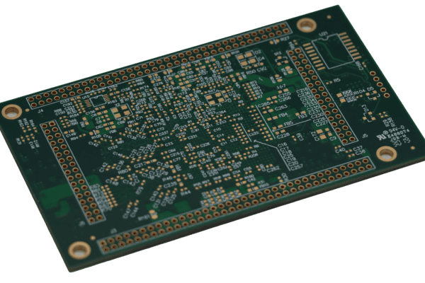
Definitions stick better with a board in hand. Take any dead electronic device, open it, and identify these features on its PCB. This is the same orientation exercise given to new electronics technicians:
1. Find the silkscreen labels. Look for printed codes: R means resistor, C capacitor, D diode, Q transistor, U integrated circuit, J connector. The numbers (R1, R2...) match the schematic.
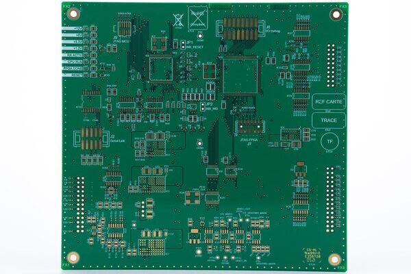
2. Trace a route. Pick a visible copper trace and follow it from one pad to another. On green boards, traces show as darker lines under the mask. You are reading the circuit's wiring.
3. Spot the vias. Tiny dots, often tinted in green, scattered across the board. Each one is a signal diving to another layer.
4. Identify the ground plane. Large unbroken copper regions, often flooding all free space. Touch points connecting to it usually have a wagon-wheel pattern (thermal relief) so pads can be soldered without the plane sinking away all the heat.
5. Check the board edge and markings. You may find the layer count, a date code, the fabricator's logo, and a UL flammability mark, plus gold-plated edge fingers if the board plugs into a slot.
Applications of PCBs Across Industries
It is difficult to find an electronic device today that does not contain at least one PCB. Here is how printed circuit boards are used across major sectors:
Consumer Electronics
Smartphones, tablets, laptops, smartwatches, TVs, game consoles, kitchen appliances, cameras, and wireless earbuds all rely on high-density multilayer and HDI PCBs.
Automotive
Modern vehicles contain dozens of PCBs — in engine control units (ECUs), infotainment systems, ADAS sensors, battery management systems (BMS), instrument clusters, and lighting controllers. Electric vehicles require especially high-performance, high-reliability boards.
Medical
Pacemakers, MRI machines, X-ray controllers, patient monitors, insulin pumps, and diagnostic imaging equipment all use PCBs — often with IPC Class 3 standards for the highest reliability.
Aerospace and Defense
Flight control systems, radar, communication equipment, satellites, and missile guidance systems use specialized high-reliability PCBs (often rigid-flex or polyimide) rated for extreme temperature, vibration, and radiation exposure.
Industrial
PLCs (Programmable Logic Controllers), motor drives, power supplies, measurement equipment, and factory automation sensors all depend on rugged industrial-grade PCBs — often with thicker copper for high-current applications.
Telecommunications
5G base stations, routers, switches, fiber optic transceivers, and antenna arrays use high-frequency RF PCBs and HDI boards to handle high-speed data transmission.
Energy and Power
Solar inverters, wind turbine controllers, battery management systems, power distribution units, and charging stations all rely on high-voltage, high-current PCB designs.
The Truth Behind 5 Common PCB Misconceptions
A few beliefs come up constantly from beginners, and each one is wrong in an instructive way:
1. "The green board is the circuit." The green is just solder mask paint. The circuit is the copper underneath and the components on top. Color choice changes nothing electrically.
2. "A PCB is a finished electronic product." A bare PCB is only the interconnection platform. It needs assembly (becoming a PCBA) and usually an enclosure, firmware, and testing before it is a product.
3. "More layers always means a better board." Layers are a tool, not a score. A well-routed 2-layer board beats a careless 6-layer board. Extra layers earn their cost only when density, signal integrity, or power delivery demand them.
4. "PCB design is just connecting the dots." Autorouters exist, yet professional designers place and route critical nets by hand, because trace geometry affects noise, heat, and reliability. The schematic defines what connects; the layout determines how well it works.
5. "Prototyping a PCB is expensive and slow." This was true twenty years ago. Today, quick-turn fabricators quote a design online in minutes and ship prototype boards in days for a few dollars each, which is why even hobbyists now order custom boards instead of hand-wiring perfboard.
From Definition to First Board: How to Get a PCB Made
Understanding what a PCB is usually leads to a practical next step, turning your own design into hardware. The path is shorter than most beginners expect:
1. Design the circuit in free or commercial EDA software. KiCad is free and fully capable; Altium is the common professional choice.
2. Run the design rule check (DRC) to catch spacing, width, and drill errors before they become physical.
3. Export Gerber and drill files, the format every fabricator accepts.
4. Get a quote and order. Modern manufacturers price boards through instant online quoting: upload the files, pick quantity, layers, thickness, and color, and see the cost immediately. For a first prototype, standard specs (2 layers, 1.6 mm, HASL finish) keep the price minimal. This is also where a manufacturer's engineering review matters more than beginners realize: platforms like PCBgogo run a free DFM (design for manufacturability) check on submitted files and flag issues such as insufficient annular rings or acid traps before production, which saves exactly the kind of respin mistakes first-time designers make.
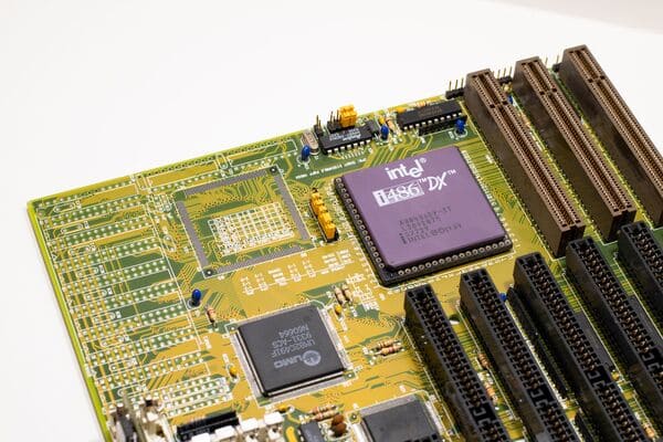
5. Choose bare board or assembly. If your parts are hand-solderable, order bare PCBs and build them yourself; it is the best way to learn. If the design uses fine-pitch chips or you need multiple identical units, a one-stop PCB plus SMT assembly order gets you tested, working boards without buying a reflow oven.
Conclusion: What a PCB Is, in One Paragraph
So, what is a PCB? It is the manufactured foundation of modern electronics: an insulating board carrying printed copper pathways that hold components in place and wire them together with photographic precision.
Whether you are building your first prototype or scaling a product to mass production, partnering with an experienced PCB manufacturer can make a significant difference in quality, turnaround time, and total cost. PCBgogo offers a streamlined digital platform for instant quoting, automated DFM review, and reliable PCB fabrication and assembly — serving engineers and companies across 200+ countries with competitive pricing and fast delivery.
If you have a PCB project on the horizon, consider uploading your Gerber files for an instant quote and free DFM check — catching design issues early saves both time and money.
FAQ: What Is a PCB?
What is a PCB in simple terms?
A PCB is a board that holds electronic components and connects them with flat copper "wires" printed onto its surface. It replaces loose wiring with a fixed, manufactured layout, which makes electronic devices smaller, cheaper, and far more reliable.
What does PCB stand for?
In electronics, PCB stands for printed circuit board. The same acronym also refers to polychlorinated biphenyls, a banned industrial chemical, in environmental contexts. The two are unrelated.
What is the difference between a PCB and a circuit board?
In everyday usage, there is none; "circuit board" is the informal name and "printed circuit board" is the full term. Strictly, "circuit board" could describe any board carrying a circuit, while PCB specifies one manufactured with printed (etched) copper wiring, which covers all modern boards essentially.
What is a PCB made of?
A standard PCB is made of an FR-4 fiberglass-epoxy substrate, one or more etched copper layers about 35 μm thick, a protective solder mask coating, and a printed silkscreen legend. Special applications substitute polyimide (flexible boards), aluminum (heat-dissipating boards), or PTFE laminates (RF boards).
Is a PCB the same as a PCBA?
No. A PCB is the bare board with no components. A PCBA is the same board after components have been soldered onto it. Only the PCBA is a functioning circuit, and suppliers quote the two as different products requiring different files.
Why are PCBs usually green?
The green color is the solder mask, and green became standard largely through historical convention and good visual contrast for inspection. Boards in blue, red, black, or white perform identically. Function never depends on color.
How much does a PCB cost?
Prototype pricing is driven by size, layer count, and quantity. A small 2-layer prototype from a quick-turn fabricator can cost only a few dollars for several copies, while multilayer, HDI, or special-material boards cost progressively more. Assembly, meaning components plus soldering, is quoted separately and typically exceeds the bare board cost several times over.
What is inside a multilayer PCB?
A multilayer PCB laminates internal copper layers between insulating prepreg sheets, all bonded into one board. Internal layers typically carry ground planes, power planes, and dense signal routing, connected to the outer layers by plated vias. A phone motherboard commonly uses 8 to 12 layers or more.





