


A correct PCB design can still run into production delays if the manufacturing package is incomplete. Missing drill data, unclear polarity markings, or an outdated BOM may force the manufacturer to stop the order and request clarification.
Preparing the right PCB file package helps your manufacturer quote accurately, review the design efficiently, and build the boards exactly as intended. Below is a practical checklist covering the files required for bare PCB fabrication and complete PCBA production.
Quick note. Not every project needs every format listed below. The exact file requested may depend on the board technology, assembly method, inspection standard, and testing requirements.
The fabrication drawing defines the mechanical and construction requirements of the bare board. It should include:
Board dimensions and outline
Finished board thickness
Hole, slot, cutout, and routing dimensions
Material and surface finish
Solder mask and silkscreen colors
Controlled-impedance requirements
Special tolerances
IPC class or acceptance standard
Any requirement that cannot be communicated clearly through Gerber or ODB++ data should appear in the fabrication drawing or its notes.
An assembly drawing shows where components, hardware, labels, and other items must be installed. Separate top- and bottom-side drawings are recommended for double-sided assemblies.
Include reference designators, component outlines, polarity indicators, connector orientations, pin-one markings, do-not-populate components, and special mounting instructions. Enlarged detail views can help clarify crowded or mechanically sensitive areas.
The bill of materials, or BOM, identifies every component needed for the assembly. A production-ready BOM normally contains:
Reference designator
Quantity
Component value and description
Package or footprint
Manufacturer name
Complete manufacturer part number
Supplier part number
Approved alternatives
DNP or DNI status
Avoid shortened part numbers and ambiguous descriptions. The BOM revision must also match the released PCB design.
Gerber RS-274X remains one of the most widely accepted PCB file formats. A complete Gerber package may contain individual files for:
Top and bottom copper
Inner copper or plane layers
Top and bottom solder mask
Top and bottom silkscreen
Top and bottom solder paste
Board outline or mechanical layer
Before uploading, inspect the files in a Gerber viewer to confirm that all layers are present, correctly aligned, and named clearly.
NC drill files define the position and diameter of vias, component holes, and mechanical holes. Depending on the design, separate files may be needed for plated holes, non-plated holes, blind vias, buried vias, or laser microvias.
The drill file should use the same units, origin, and coordinate format as the Gerber data. A drill drawing or tool table is also useful for confirming finished hole sizes and tolerances.
The pick-and-place file - also called centroid, XY, or placement data - guides automated component placement equipment. It should include:
Reference designator
X and Y center coordinates
Rotation angle
Top or bottom board side
Package or part number
Confirm the coordinate origin and rotation convention before release. For polarized parts, the placement data should agree with the assembly drawing and silkscreen.
Download Pick & Placement Template
ODB++ is an intelligent manufacturing format that can combine layer artwork, drill information, net data, component placement, and other design details in one structured package. This reduces the risk of mismatched files and gives CAM engineers more data for design-for-manufacturing checks.
When ODB++ is supplied, confirm whether the manufacturer still wants separate drawings, a BOM, or other supporting documents.
The stackup drawing describes the physical construction of a multilayer PCB. It should specify the order of copper and dielectric layers, core and prepreg materials, copper weights, finished thickness, and impedance targets.
For controlled-impedance, high-speed, RF, HDI, flex, or rigid-flex designs, the stackup should be reviewed with the manufacturer before the layout is finalized.
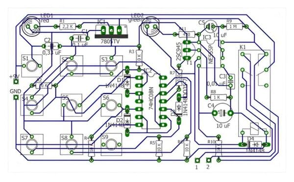
A netlist records the intended electrical connections between pads and component pins. An IPC-D-356 netlist is particularly useful for independent bare-board electrical verification and for identifying possible opens or shorts.
Although a netlist may not always be mandatory, supplying one gives the manufacturer an additional reference that is independent of the Gerber artwork.
Assembly drawings show where parts belong; schematics explain how they connect and function. Used together, they help engineers verify component polarity, resolve discrepancies, understand special circuits, and troubleshoot boards during testing.
These documents support the BOM and placement data but should not replace them.
Complex or reliability-sensitive assemblies may require additional documentation:
ICT requirements: Test-point locations, net access, acceptable limits, fixture details, and test coverage targets.
X-ray inspection requirements: Components requiring inspection, such as BGA, QFN, or LGA devices, together with acceptance criteria for voids, alignment, and hidden solder joints.
Assembly process instructions: Solder alloy, reflow profile, selective or hand-soldering steps, component height limits, cleaning, conformal coating, and special handling requirements.
Functional test documents: Test procedures, firmware, programming files, fixtures, cables, expected results, and pass/fail limits.
Mechanical data: STEP models and enclosure drawings for checking connector positions, clearances, and overall fit.
Compliance information: RoHS, REACH, traceability, IPC class, material restrictions, or industry-specific requirements.
Golden sample: An approved assembly that can serve as a workmanship and functional reference.
Only include documents relevant to the build, and make sure every file carries a consistent part number and revision.
Once the documentation is ready, using one supplier for fabrication, component sourcing, assembly, and inspection can simplify revision control and communication.
PCBgogo accepts common formats including Gerber RS-274X, ODB++, IPC-2581, Altium .PcbDoc, Protel PCB, and EAGLE files. For PCBA orders, the core package includes the PCB design data, BOM, and pick-and-place file. Schematics, 3D data, and assembly drawings can be added when the design needs further clarification. View PCBgogo file requirements
Its PCB services cover standard and advanced technologies, including FR-4 boards with up to 40 layers, HDI structures, blind and buried vias, rigid, flex, rigid-flex, metal-core, and controlled-impedance designs. Explore PCB manufacturing capabilities
For assembly, PCBgogo handles SMT, through-hole, and mixed-technology projects, with turnkey, partial-turnkey, and consigned component options. Its published capabilities include 01005 components, fine-pitch BGA assembly, AOI, X-ray inspection, functional testing, and free DFM checks. Prototype orders can start from one piece, making the service suitable for both engineering validation and volume production. Review PCBA capabilities
Ready for production? Prepare one revision-controlled package, then upload your design for engineering review and quotation.
A reliable production package does more than describe the PCB - it removes uncertainty. Gerber or ODB++ data defines the board, drill files define the holes, and the BOM, pick-and-place file, assembly drawings, and schematics guide assembly.
Before submitting an order, check that every PCB file belongs to the same revision, uses a common origin, and contains no conflicting instructions. A few minutes spent reviewing the package can prevent days of avoidable delay.
For a standard bare PCB, manufacturers generally need Gerber files and NC drill files. A fabrication drawing, stackup, and netlist should be added when the board has special mechanical, material, impedance, or testing requirements.
A typical PCBA order requires PCB production data, a BOM, and a pick-and-place file. Assembly drawings and schematics are strongly recommended for polarized, non-standard, or densely populated designs.
Yes, many manufacturers can produce a board directly from ODB++. However, drawings, BOM data, special process instructions, and test requirements may still be requested separately.
The additional file requested usually contains information that cannot be confirmed from the existing data, such as component orientation, finished hole size, material construction, impedance, or test criteria.
Yes. Use clear filenames, remove obsolete versions, include a revision identifier, and review the complete archive before uploading it for quotation or production.

 日本語
日本語
 한국어
한국어

