
 日本語
日本語
 한국어
한국어

How to Create Gerber Files? Complete Guide for Popular PCB Tools
If you have ever sent a PCB design to a manufacturer and received boards that did not match your design, the problem may have started with the Gerber files. Gerber files contain the production data used to manufacture your PCB. They are different from the original design files. Exporting them correctly is essential to prevent manufacturing errors, delays, and costly rework.
This guide explains how to generate Gerber files in Altium Designer, KiCad, Autodesk EAGLE, and Cadence Allegro (OrCAD). It also covers what Gerber files are, common export mistakes, and what to check before placing an order. Following these guidelines can help you submit accurate production files and improve the chances of getting your PCB right the first time.
What Is a Gerber File?
A Gerber file is a 2D vector format used for PCB manufacturing. It describes each layer of a circuit board in a format that fabrication equipment can read. These layers include the top and bottom copper, solder mask, silkscreen, and board outline. Drill data is usually provided in a separate file.
You do not need to send the original Altium Designer, KiCad, or EAGLE project files to your PCB manufacturer. Instead, export a complete set of Gerber and drill files. These files contain the production data needed to manufacture your board according to your design.
Two Gerber formats are in common use today. RS-274X embeds aperture definitions directly in each layer file and is the current industry standard. Gerber X2 is a newer extension of RS-274X that adds layer-stackup and net attribute data, giving fabricators more automated design-for-manufacturing checks. Most modern fab houses accept either, but it's worth confirming with your manufacturer before export, since a small number of shops still expect the older RS-274-D format.
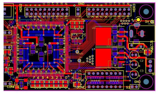
Now that you know what Gerber files are, the next step is to export them correctly from your PCB design software. Some manufacturers can create production files from your original project files. However, exporting the Gerber files yourself gives you more control over the final output.
Settings such as layer selection, units, coordinate format, and Gerber version can affect the production data. Differences in software or export settings may lead to missing layers, incorrect dimensions, or other manufacturing issues.
Generating and reviewing your own Gerber files helps ensure that the production data matches your design. The following sections explain how to export Gerber files from several popular PCB design tools.
How to Generate Gerber Files in Altium Designer
Altium Designer is a common choice for professional and enterprise PCB teams, and its Gerber export is handled through a dedicated setup dialog with five configuration tabs.
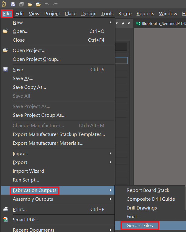
Step 1: Open the Gerber setup. With your.PcbDoc file open, go to File > Fabrication Outputs > Gerber Files. This opens the Gerber Setup dialog.
Step 2: Set units and format. On the General tab, choose Inches or Millimeters and select a coordinate format. A 2:5 format gives higher resolution than 2:3, and either is fine for most boards as long as it's consistent with your drill file.
Step 3: Select your layers. On the Layers tab, tick every layer you want plotted (and mirrored, if needed). Leave mechanical layers unchecked unless your fabricator specifically requests them.
Step 4: Review drill drawing settings. The Drill Drawing tab rarely needs changes — the default legend settings work for most designs.
Step 5: Confirm the aperture format. On the Apertures tab, make sure Embedded Apertures (RS274X) is checked. This keeps aperture data inside each layer file rather than requiring a separate aperture file.
Step 6: Set advanced options. On the Advanced tab, leave Film Size on its default, set Aperture Matching Tolerances to 0.005mil for both Plus and Minus, and choose Separate file per layer under Batch Mode. Match Leading/Trailing Zeroes and Position on Film to whatever you'll use for your NC Drill files.
Step 7: Generate the files. Click OK. Altium exports a separate Gerber file for each selected layer to your project's output folder.
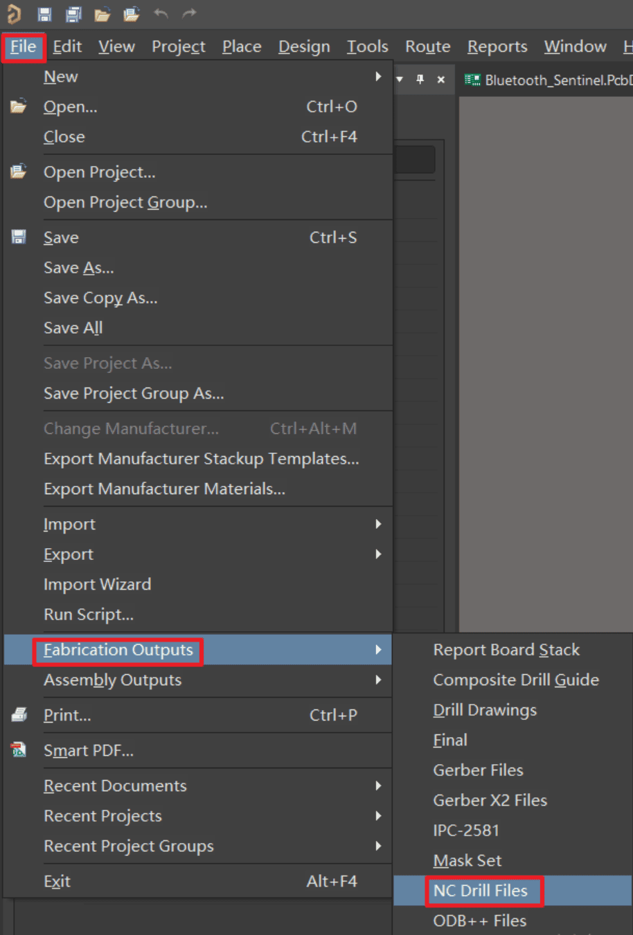
Don't forget the drill data: File > Fabrication Outputs > NC Drill Files generates the corresponding Excellon drill file separately, and both sets need to be zipped together before you send them off.
How to Generate Gerber Files in KiCad
KiCad is free and open-source, and it's become one of the most widely used PCB tools for hobbyists, students, and startups — which makes its Gerber workflow worth knowing well even though it's less frequently covered in manufacturer guides.
Step 1: Run a design rule check first. Before exporting anything, run DRC (Inspect > Design Rules Checker) and refill copper zones (Edit > Fill All Zones, or press B). Stale zone fills are one of the most common causes of incorrect Gerbers.
Step 2: Open the Plot dialog. In Pcbnew, go to File > Fabrication Outputs > Gerbers (.gbr), or click the Plot icon in the toolbar.
Step 3: Set your output folder and layers. Choose a dedicated output directory (KiCad will create it if it doesn't exist), then select the layers to include: F.Cu, B.Cu, F/B.Paste, F/B.Silkscreen, F/B.Mask, Edge.Cuts, and any inner copper layers for 4+ layer boards.
Step 4: Configure plot options. Enable Check zone fills before plotting, Plot footprint values (if needed), and Use extended X2 format if your fabricator supports it — leave it unchecked for standard RS-274X.
Step 5: Plot the Gerbers. Click Plot. KiCad generates one file per selected layer in your chosen folder.
Step 6: Generate drill files. From the same Plot window, click Generate Drill Files, select Excellon format, match your drill units to your design units, and click Generate Drill File.
Step 7: Verify before sending. Open the exported files in KiCad's Gerber Viewer (or any third-party viewer) to confirm the board outline is fully closed and every layer looks correct before zipping and submitting.
How to Generate Gerber Files in Autodesk EAGLE
EAGLE exports Gerbers through its CAM Processor, using a CAM job file that defines which layers map to which output files.
Step 1: Run the drill configuration ULP. Open your .brd file, go to File > Run ULP, and select drillcfg.ulp to generate the drill configuration before exporting.
Step 2: Open the CAM Processor. Go to File > CAM Processor (or click the CAM icon on the toolbar).
Step 3: Load a Gerber job file. Select File > Open > Job and load a CAM job such as gerb274x.cam. Most fabricators publish a ready-made CAM file for EAGLE, which is worth using since it's pre-configured for their equipment.
Step 4: Check your silkscreen and outline layers. By default, EAGLE only exports the top silkscreen — add the bottom silkscreen layers manually if your design needs it. Confirm your board outline is drawn as a closed shape on the Dimension layer, since a missing or open outline is one of the most common EAGLE export errors.
Step 5: Process the job. Click Process Job. EAGLE generates the Gerber files (and, in recent versions, packages them into a single ZIP automatically).
Step 6: Generate the drill file. Reopen the CAM Processor, load excellon.cam, and process it separately to produce your drill file.
Step 7: Verify layer-by-layer. Use EAGLE's built-in Gerber preview in the CAM Processor, or an external viewer, to check each layer before compressing everything into a single ZIP for submission.
How to Generate Gerber Files in Cadence Allegro (OrCAD)
Allegro is common on high-layer-count and high-complexity boards, and its Artwork Control Form handles Gerber generation for the full stackup at once.
Step 1: Open the Artwork Control Form. With your layout open in Allegro, go to Manufacture > Artwork.
Step 2: Add a board outline film. Right-click the TOP folder in the film list and choose Add Manual, name it (for example, OUTLINE), and click OK.
Step 3: Assign the outline subclass. In the Subclass Selection window, expand BOARD GEOMETRY, check OUTLINE, and click OK.
Step 4: Confirm the film is active. Back in the Artwork Control Form, make sure OUTLINE appears and is checked under Available films.
Step 5: Select all layers. Click Select All so every required layer is included in the output.
Step 6: Generate the artwork. Click Create Artwork. Allegro writes a Gerber file for each selected layer to your working directory.
As with the other tools, generate your NC drill data as a separate step and confirm both sets use matching units and origin before zipping them together for your fabricator.
Software Comparison at a Glance
| Software | Cost | Native File | Gerber Format | Best For |
|---|---|---|---|---|
| Altium Designer | Paid (subscription) | .PcbDoc | RS-274X / Gerber X2 | Professional & enterprise teams |
| KiCad | Free, open-source | .kicad_pcb | RS-274X / Gerber X2 | Hobbyists, startups, students |
| Autodesk EAGLE | Free tier + paid tiers | .brd | RS-274X (via CAM job) | Makers, small-team production boards |
| Cadence Allegro (OrCAD) | Paid (enterprise) | .brd | RS-274X | High-layer-count, complex designs |
Common Errors to Avoid When Generating Gerber Files
Exporting with stale copper zones — always refill zones and re-run DRC immediately before export.
Leaving the board outline (Edge.Cuts / Dimension / Keep-Out layer) open or incomplete, which prevents the fabricator from routing the board correctly.
Mismatched units or origin points between your Gerber and drill files, which causes misregistration between copper and holes.
Forgetting inner copper layers on 4+ layer boards.
Mixing Gerber X2 and legacy RS-274X settings without confirming your fabricator supports the format you chose.
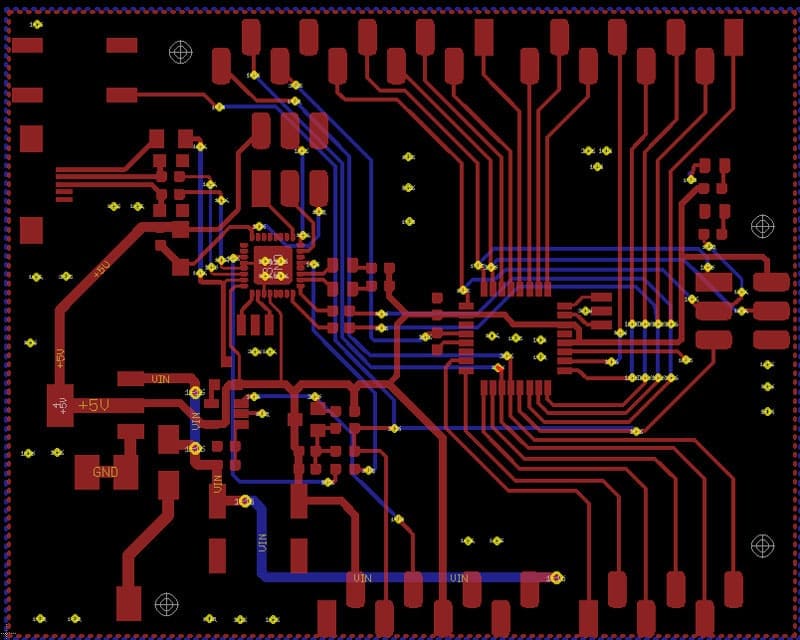
Sending files without opening them in a Gerber viewer first — a five-minute check catches most avoidable respins.
Pre-Submission Checklist
DRC passed with zero unresolved errors
All copper zones refilled
Board outline forms a single closed shape
Correct layer count exported, including inner layers
Units and origin match between Gerber and drill files
Files reviewed in a Gerber viewer
All files (Gerbers + drill + drill map) zipped together in one archive
Getting Your Gerber Files Manufactured
Once your Gerber files are exported and verified, the next step is to upload them to a PCB manufacturer and move into production with confidence that your design is correctly interpreted. You can directly submit your files to PCBgogo, where they are automatically checked through a design-for-manufacturing (DFM) review before fabrication begins, helping catch potential issues like outline errors, spacing problems, or missing layers at an early stage.
PCBgogo Capabilities for Gerber-Based Orders
Founded in 2013, ISO 9001:2015 & UL certified → ensuring standardized quality control and manufacturing reliability.
Free DFM checks on uploaded Gerber files → automatically detect issues such as open outlines, incorrect stackups, or missing drill data before production starts.
HDI fabrication capabilities → enabling high-density, fine-pitch designs beyond standard PCB complexity.
Precision SMT assembly with X-ray inspection → supporting BGA and other hidden-joint components for higher assembly accuracy.
1-board minimum order → flexible enough for rapid prototyping while still supporting small-scale production runs.
Whichever design tool you use, the workflow remains consistent: export clean Gerber and drill files, verify them carefully, then upload directly to the manufacturer's online quoting system for DFM review and production.
Frequently Asked Questions
What is a Gerber file used for?
A Gerber file describes a single layer of a PCB — copper, solder mask, silkscreen, or drill data — in a standardized vector format that PCB fabrication equipment reads directly to manufacture the board and, when applicable, its assembly stencils.
What's the difference between RS-274X and Gerber X2?
RS-274X embeds aperture data in each layer file and is the current baseline standard accepted by virtually all fabricators. Gerber X2 extends RS-274X with additional layer-stackup and net attribute information, enabling more automated checks on the fabricator's side. Most shops accept either format, but it's worth confirming before export.
Do I need to generate Gerber files myself, or can my manufacturer do it from my design file?
You should generate them yourself whenever possible. Manufacturers may use different design or CAM software than you do, and letting someone else configure the export removes your control over units, layers, and format — details that directly affect whether the finished board matches your design.
How many Gerber files does a PCB need?
Each layer of the board — top and bottom copper, solder mask, silkscreen, paste layers, and board outline — needs its own Gerber file, plus a separate drill file for hole data. A simple two-layer board typically produces around seven to ten files; multilayer boards produce more, one set per inner copper layer.
Can I preview my Gerber files before sending them to a manufacturer?
Yes. Most design tools include a built-in Gerber viewer (KiCad's Gerber Viewer, EAGLE's CAM Processor preview), and free standalone viewers are also widely available. Reviewing every layer before submission is one of the most effective ways to catch outline, layer, or registration errors ahead of fabrication.





