Electronic Project Engineer's Best Partner!
Online Quote
Upload Gerber File
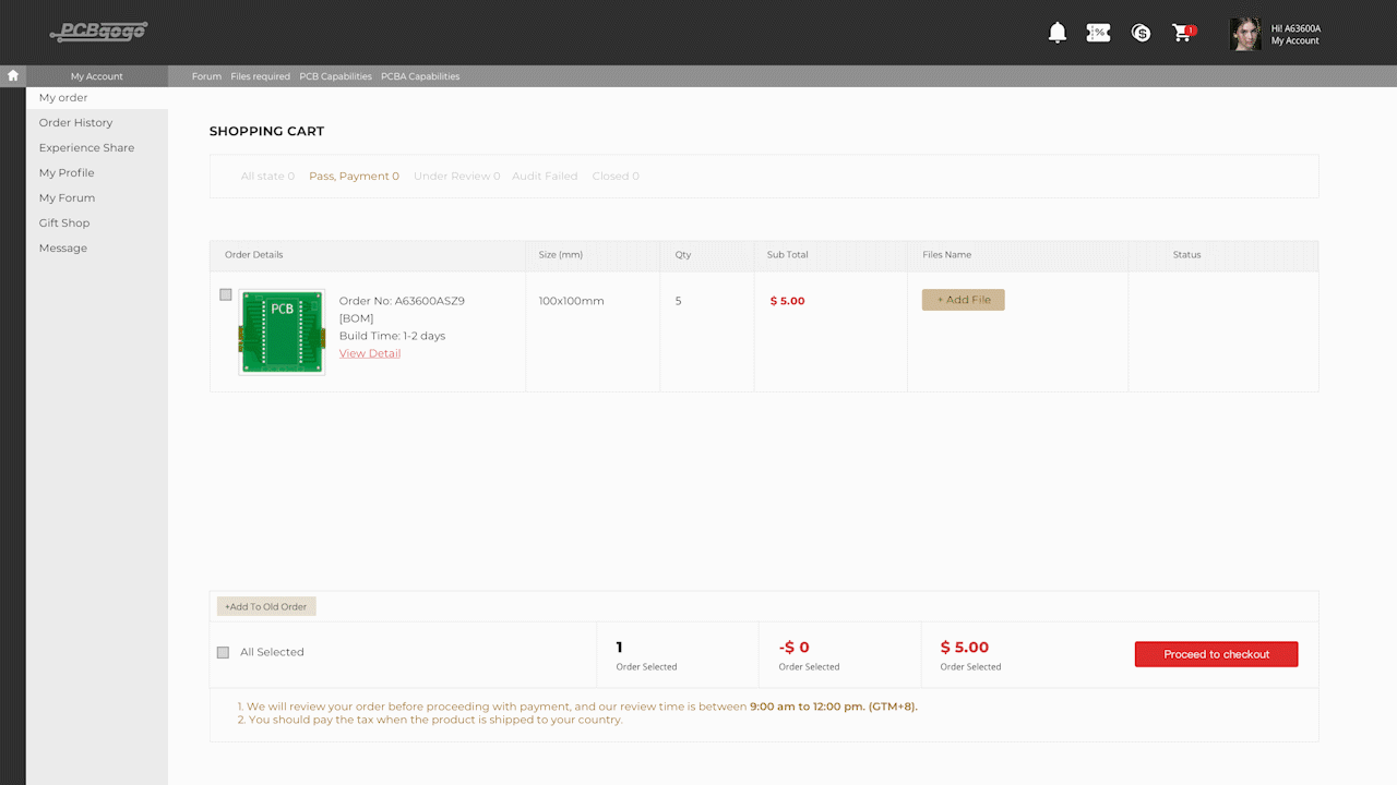
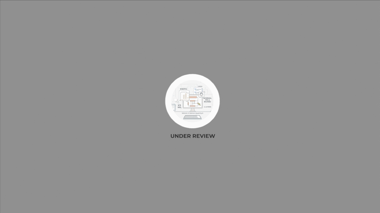
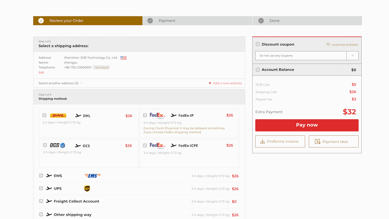
Order review
Payment
Fabrication
Shipment
Confirm and Review


Please fill in the layer order from top to bottom here.

Please fill in the layer order from top side view tobottom side according to
the layers name in your file.
Submit
QUICK CONTACT
Please leave your message below and one of our helpful staff will contact you within 48 hours.
Whatsapp: +8618665922549
Email: service@pcbgogo.com
Tel: +86 - (0) 755-2330-0601
- OTHERS
- RoHS-lead Free PCBs
- Online Gerber View
- Automated Optical Inspection (AOI)
- Automated X-ray inspection (AXI)
- Quality guarantee
- Electric Test (E-test)
- HELP & CONTACT
- Help center
- Contact Us
- Sign In / Register
- PCBGOGO SERVICES/PRODUCT
- PCB Instant Quote
- PCB Assembly service
- Advanced PCB
- Flex / Rigid-flex PCB
- Multilayer PCB
- Online Quote
- Upload PCB File
- Order Review
- Payment