



 日本語
日本語
 한국어
한국어

PCB vs PCBA: Key Differences in Manufacturing, Cost & Buying
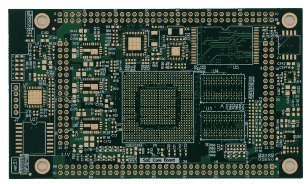
A PCB (printed circuit board) is the bare board with copper traces, pads, and vias on an insulating substrate, with no components mounted. A PCBA (printed circuit board assembly) is that same board after resistors, capacitors, ICs, and connectors have been soldered onto it, making it a functional circuit. In short: PCB + components + soldering = PCBA. A PCB cannot perform any electronic function on its own while a PCBA is capable of that.
Even though these brief explanations clearly distinguish PCB from PCBA from a definitional standpoint, they hardly address cost?related choices we regularly deal with in real?world projects. From my years working as a PCB manufacturing engineer, I’ve noticed engineers and procurement specialists always face follow?up practical concerns. They frequently wonder whether they should purchase bare?circuit boards or finished assembled versions, which document files each option demands, and why PCBA pricing runs four to ten times higher than a plain?PCB quote for identical board layouts. Drawing on my on?the?job experience, I put together this guide. It walks you through core aspects including official definitions, production workflows, cost?composition breakdowns, qualification testing criteria, production turnaround cycles, and practical judgment guidelines to help you pick the suitable option.
What Is a PCB (Printed Circuit Board)?
A printed circuit board is the physical foundation of nearly every electronic device. It consists of one or more conductive copper layers laminated onto an insulating substrate, most commonly FR-4 fiberglass epoxy, though polyimide (for flex circuits), aluminum (for LED and power applications), and PTFE-based laminates (for RF designs) are also used.
A bare PCB provides two things:
1. Mechanical support: a rigid (or flexible) platform where components will later be mounted.
2. Electrical interconnection: etched copper traces, pads, and plated through-holes or vias that route signals and power between component locations.
What a bare PCB does *not* provide is function. When you power it up and nothing happens, there are no active or passive components to process signals. This is why a PCB is sometimes described as the skeleton of an electronic product, for the structure is complete, but nothing is alive yet.
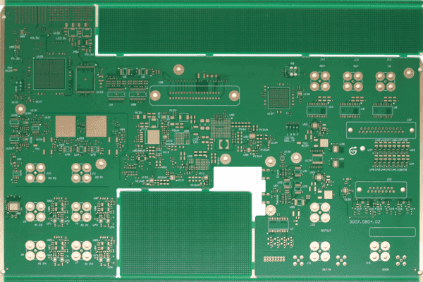
Key elements of a bare PCB
Substrate (core and prepreg): the insulating base material that determines rigidity, thermal performance, and dielectric properties.
Copper layers: from a single layer up to 20+ layers in high-density designs; standard outer-layer copper weight is 1 oz (35 μm), with heavy copper options for high-current boards.
Solder mask: the polymer coating (typically green, but also blue, red, black, or white) that protects copper and prevents solder bridging during assembly.
Silkscreen: printed reference designators (R1, C3, U2) and polarity marks that guide assembly and debugging.
Surface finish: HASL, lead-free HASL, ENIG, OSP, or immersion silver/tin. These finishes get applied to exposed pads so they stay solderable until assembly.
One detail worth noting: the surface finish on a bare PCB exists almost entirely *for the sake of the future PCBA*. Copper oxidizes within hours of exposure; the finish preserves solderability during the weeks between board fabrication and component assembly. This is also why bare PCBs are vacuum-sealed with desiccant for shipping. It marks a packaging difference from PCBAs, which ship in anti?static (ESD) bags or trays to protect the mounted semiconductors instead.
What Is a PCBA (Printed Circuit Board Assembly)?
A printed circuit board assembly is the bare PCB after the assembly process is complete: solder paste applied, components placed, solder joints reflowed or wave-soldered, and the finished board inspected and tested. The term PCBA is used in two related ways:
As a noun: the assembled board itself — the semi-finished product that goes into an enclosure to become a final device.
As a process: "PCBA" or "PCB assembly" describing the manufacturing service of populating boards.
You may also encounter CCA (circuit card assembly), common in aerospace and defense documentation, and the legacy term PWB/PWA (printed wiring board/assembly) still used in Japan and in older standards. Functionally, CCA and PCBA refer to the same thing. Knowing these synonyms matters when reading datasheets, military specs, or supplier quotes because vocabulary changes while the actual object stays unchanged.
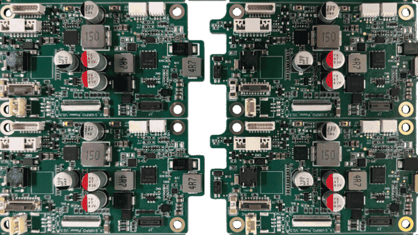
A PCBA is not usually the end product. A smartphone motherboard serves as a PCBA, and the smartphone combines this PCBA with a display, battery, enclosure, and firmware. Industry professionals refer to this later-stage process as box build or system integration.
PCB vs PCBA: Difference at a Glance
The table below summarizes the PCB vs PCBA difference across every dimension buyers and engineers actually compare:
| Dimension | PCB (Bare Board) | PCBA (Assembled Board) |
|---|---|---|
| Definition | Unpopulated board with copper traces, pads, and vias | PCB with all electronic components soldered on |
| Functionality | No electronic function; provides structure and interconnection only | Fully functional circuit, ready for firmware or box build |
| Manufacturing Scope | Fabrication: imaging, etching, lamination, drilling, plating, solder mask, and surface finish | PCB fabrication + solder paste printing, component placement, reflow/wave soldering, and inspection |
| Files Required to Order | Gerber files (or ODB++) + drill files | Gerber files + BOM (Bill of Materials) + centroid/pick-and-place file |
| Inspection Standard | IPC-A-600 (acceptability of printed boards); electrical test per IPC-9252 | IPC-A-610 (acceptability of electronic assemblies); solder joints per J-STD-001 |
| Typical Testing | E-test (flying probe or bed-of-nails continuity/isolation), AOI on traces | SPI, AOI, X-ray inspection (for BGA/QFN), ICT, and functional testing |
| Cost Structure | Material + fabrication process + tooling (NRE) | PCB cost + component cost + stencil + assembly labor/machine time + testing |
| Relative Cost | Lower — often 10–30% of the equivalent PCBA price | Higher — components frequently account for 50–70% of total PCBA cost |
| Typical Prototype Lead Time | 24 hours – 5 days | PCB lead time + 3–10 days for parts sourcing and assembly |
| Packaging | Vacuum-sealed with desiccant to preserve solderability | Anti-static (ESD) bags, foam, or trays to protect components |
| Who Typically Buys It | Teams with in-house assembly, hand-solder prototypers, and educational users | Product companies, startups without SMT lines, and customers needing turnkey delivery |
In-Depth Analysis of Core Differences Between PCB and PCBA
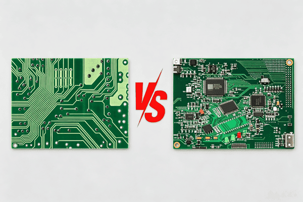
1. Different Production Stages
PCB fabrication is the first step of electronic board production, belonging to the primary manufacturing link. It only completes the production of the circuit carrier and does not involve any component assembly work. PCBA is the secondary processing link based on qualified PCBs, which is the final key step to realize product functions.
There is an inevitable sequential relationship between the two: there can be no PCBA without a qualified PCB. The quality of bare PCB directly determines the yield rate of subsequent PCBA assembly.
2. Different Technical Difficulties
PCB manufacturing focuses on precision control of circuits, vias, and layers. Multi-layer boards, high-density wiring, and special substrate materials require high-precision production equipment and process technology.
PCBA processing pays more attention to assembly precision, component compatibility, and soldering quality. For high-precision components such as BGA and 0201 ultra-small patches, manual assembly is almost impossible, and fully automated SMT equipment and professional process debugging are required.
3. Different Project Costs
Bare PCB has a single cost composition and low prototype cost, which is very suitable for early-stage repeated debugging by developers. However, if you need to purchase components and find assembly manufacturers separately, the comprehensive time cost and logistics cost will increase significantly.
Although the unit price of PCBA is higher than that of bare PCB, the turnkey one-stop service like PCBgogo can effectively save component procurement costs, multi-vendor communication costs, and assembly debugging costs. It is the most cost-effective solution for small-batch and mass production projects.
PCB Manufacturing vs PCBA Manufacturing: Two Different Processes
The clearest way to understand PCB manufacturing vs PCBA manufacturing is to see them as sequential stages run on entirely different equipment, judged by different quality standards, and quoted with different pricing logic.
How a bare PCB is manufactured
PCB fabrication is a subtractive chemical and mechanical process. For a standard multilayer board:
1. Inner layer imaging and etching — the circuit pattern is transferred photolithographically onto copper-clad laminate, and unwanted copper is etched away.
2. Lamination — inner layers, prepreg, and copper foil are stacked and bonded under heat and pressure into a single multilayer panel.
3. Drilling — mechanical or laser drilling creates through-holes, blind vias, and buried vias.
4. Plating — electroless and electrolytic copper plating metallizes hole walls, connecting layers electrically.
5. Outer layer imaging and etching — the outer circuit pattern is formed.
6. Solder mask and silkscreen — protective coating and legend printing.
7. Surface finish — HASL, ENIG, or OSP applied to exposed pads.
8. Profiling and electrical test — routing/V-scoring to final shape, then 100% continuity and isolation testing (flying probe for prototypes, test fixtures for volume).
The quality benchmark at this stage is IPC-A-600 (visual/dimensional acceptability of bare boards) and IPC-6012 (qualification and performance of rigid boards). If a fabricator can state which IPC-6012 class it builds to — Class 2 for standard commercial products, Class 3 for high-reliability applications — that's a meaningful signal of process control.
How a PCBA is manufactured
PCB assembly is an additive placement-and-soldering process, dominated today by SMT (surface-mount technology), with THT (through-hole technology) used for connectors, large electrolytics, and mechanically stressed parts:
1. Solder paste printing — paste is applied through a laser-cut stainless stencil onto SMT pads.
2. SPI (solder paste inspection) — 3D measurement of paste volume and alignment; most solder defects trace back to this step, which is why serious assemblers inspect here rather than only at the end.
3. Pick-and-place — machines place components at rates of tens of thousands of parts per hour, from 01005 chip resistors to large BGAs.
4. Reflow soldering — the board passes through a multi-zone oven with a controlled thermal profile that melts the paste and forms joints.
5. AOI (automated optical inspection) — camera-based verification of presence, polarity, and joint quality.
6. X-ray inspection — required for hidden-joint packages like BGA and QFN, where optical inspection physically cannot see the solder.
7. THT insertion and wave/selective soldering — for through-hole parts.
8. ICT and functional testing — in-circuit test verifies individual component values and connections; functional test powers the board and validates real behavior.
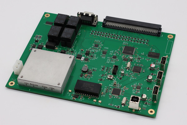
Here the governing standards shift to IPC-A-610 (acceptability of electronic assemblies) and J-STD-001 (soldering requirements). This standards handoff — IPC-A-600 for the board, IPC-A-610 for the assembly — is a detail worth remembering: it means a "passed" bare PCB can still yield a failed PCBA if the assembly process is poorly controlled, and vice versa, a perfect assembly line cannot rescue a defective bare board.
Cost Difference Between PCB and PCBA: What You're Actually Paying For
The price gap between a bare PCB quote and a PCBA quote surprises many first-time buyers. It shouldn't — the two quotes cover different scopes.
A bare PCB quote covers: laminate material, fabrication processing (scaled by layer count, board size, quantity, and special features like impedance control or via-in-pad), tooling/NRE, and electrical test. For a simple 2-layer prototype, this can be just a few dollars per board; a 6-layer board with controlled impedance costs more but remains modest at prototype quantities.
A PCBA quote adds: every component on the BOM (frequently 50–70% of total assembled cost, dominated by a handful of ICs), a laser-cut stencil (one-time), SMT machine programming and setup (one-time per revision), placement cost per joint or per component, THT hand-soldering labor if applicable, and inspection/test time.
Three practical cost rules follow from this structure:
Setup costs amortize with volume. At 5 boards, stencil and programming dominate and per-unit price looks painful. At 500 boards, those same fixed costs become negligible. This is why PCBA unit prices fall much more steeply with quantity than bare PCB prices do.
The BOM, not the assembly, is usually the cost lever. If an assembled board is over budget, reviewing component selection (do you need that ±0.1% resistor? is there a cheaper pin-compatible MCU?) typically saves more than negotiating assembly rates.
Design revisions cost more after assembly. Scrapping a batch of bare PCBs due to a design error wastes board cost only. Scrapping assembled boards wastes boards *plus* components *plus* labor. This asymmetry is exactly why prototyping practice orders small PCBA runs before committing to volume.
When to Order a Bare PCB vs a PCBA: Decision Framework
Choosing between ordering bare printed circuit boards and ordering printed circuit board assemblies comes down to four questions:
1. Do you have assembly capability? If your team has reflow equipment, skilled hand-soldering, and time — or the design uses only large, hand-solderable packages — bare PCBs plus self-assembly can work for early prototypes. If the design includes BGA, QFN, or 0402-and-smaller passives, hand assembly becomes unreliable, and professional SMT assembly is the practical route regardless of quantity.
2. What stage is the project in? Early breadboard-replacement prototypes where you expect to cut traces and bodge wires favor bare boards you can modify freely. Design-validation prototypes meant to represent the real product favor PCBA, because assembly quality itself is part of what you're validating.
3. Who should own component sourcing? This defines the three standard PCBA procurement models:
Full turnkey: the manufacturer fabricates the boards, sources all components, and assembles. One vendor, one point of accountability, fastest for teams without purchasing infrastructure.
Consignment: you supply all components; the vendor assembles only. Sensible when you hold inventory or use long-lead parts you've already secured.
Partial turnkey: you supply critical or pre-purchased parts (often the main IC); the vendor sources the commodity passives. The most common compromise in practice.
4. How tight is the schedule? Splitting fabrication and assembly across two vendors adds a shipping-and-handoff step and, more importantly, splits responsibility — if assembled boards fail, the fabricator and assembler can each point at the other. A combined PCB + assembly order under one roof removes that gap, which is a major reason one-stop manufacturers exist.
Platforms like PCBgogo, which support full turnkey, consignment, and partial turnkey procurement models, allow customers to choose the sourcing approach that best fits their project needs. With PCB fabrication, component sourcing, and SMT assembly integrated into a single quoted workflow, PCBgogo helps prototype and small-batch buyers simplify DFM review, manufacturing coordination, and production management through one accountable supplier.
Common Mistakes When Buying PCBs/PCBAs and How to Avoid Them
These are the errors that show up repeatedly in real procurement, each avoidable with one habit:
Mistake 1: Ordering a "PCB" and expecting an assembled board. Because some listings and even suppliers use the terms loosely, buyers occasionally receive bare boards when they needed functional units. Fix: confirm scope explicitly — if your quote doesn't itemize a BOM and assembly, you are buying bare boards.
Mistake 2: Submitting a BOM with incomplete part numbers. A BOM line reading "10uF capacitor" without a manufacturer part number forces the assembler to guess voltage rating, dielectric, and package — a leading cause of quote delays and wrong-part assembly. Fix: every BOM line needs a full MPN, quantity, and reference designators; note approved alternates in advance.
Mistake 3: Skipping the centroid file. Gerbers alone cannot tell a pick-and-place machine where component centers and rotations are. Fix: export the centroid (pick-and-place/XY) file from your EDA tool with every assembly order.
Mistake 4: Ignoring DFM/DFA feedback. Design-for-manufacturing issues (acid traps, insufficient annular rings) and design-for-assembly issues (parts too close to the board edge, mixed-orientation polarized parts) are cheap to fix before production and expensive after. Fix: treat the manufacturer's engineering questions as free consulting, not friction. A supplier that runs a genuine DFM review before fabrication — rather than building whatever arrives — is materially reducing your respin risk.
Mistake 5: Validating volume pricing with prototype specs. Prototype pricing and volume pricing scale differently for PCB and PCBA (see cost section above). Fix: when comparing suppliers, quote your realistic production quantity, not just 5 pieces.
Mistake 6: No test requirement in the assembly order. "Assembled" does not automatically mean "tested beyond AOI." Fix: specify inspection standard (IPC-A-610 Class 2 or 3) and whether you need X-ray for BGAs, ICT, or functional testing — and expect the supplier to document results.
From Bare PCB to Finished Product: Where Each Fits in the Manufacturing Chain
Understanding the full sequence clarifies why both terms exist and why neither replaces the other:
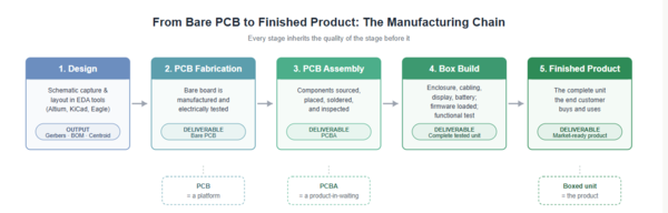
Design → PCB fabrication → PCB assembly (PCBA) → box build → finished product
Design: schematic capture and layout in EDA tools (Altium, KiCad, Eagle), producing Gerbers, BOM, and centroid files. Since the PCB design software you choose can greatly affect your workflow and design efficiency, we've put together a guide to the best PCB design software to help you find the right tool for your needs.
PCB fabrication: the bare board is manufactured and electrically tested. Deliverable: bare PCB.
PCB assembly: components are sourced, placed, soldered, and inspected. Deliverable: PCBA.
Box build: the PCBA is integrated with enclosure, cabling, display, battery; firmware is loaded; the complete unit is functionally tested.
Finished product: what the end customer buys.
A useful mental model: the PCB is a platform, the PCBA is a product-in-waiting, and the boxed unit is the product. Every stage inherits the quality of the stage before it — which is the deepest practical reason the PCB vs PCBA distinction matters. A signal-integrity problem baked into the bare board cannot be soldered away during assembly, and a flawless bare board cannot survive a badly profiled reflow oven.
How to Choose a Reliable PCB & PCBA Manufacturer?
The quality of PCB and PCBA directly determines the stability and service life of electronic products. Many developers face problems such as uneven product quality, hidden charges, delayed delivery, and unguaranteed after-sales when choosing manufacturers. A professional and reliable manufacturing partner needs to have formal qualifications, complete production lines, standardized testing processes and transparent pricing rules.
For global electronics developers and small and medium-sized enterprises, PCBgogo has become a trusted one-stop PCB & PCBA manufacturing service provider relying on its self-built factory and mature industrial system. As a professional electronic manufacturing brand focusing on global markets, PCBgogo has standardized production plants, with complete ISO9001, UL, RoHS, CE and other international certifications.
Different from manufacturers with a single business, PCBgogo supports full-link services including bare PCB prototyping, multi-layer board mass production, SMT/DIP assembly, global component sourcing, and finished board testing. It solves the pain points of difficult component matching, multi-vendor communication troubles, and inconsistent front and back process quality for developers.
In terms of service efficiency and cost control, PCBgogo provides real-time online quotation with no hidden fees, supports 1-piece prototype customization and 24-hour accelerated PCB production, and provides free DFM design inspection to help users avoid design defects and reduce production risks. Serving more than 200 countries and regions around the world, it has stable cross-border logistics and a perfect after-sales system, which is very suitable for R&D engineers and small-batch production enterprises who pursue high cost performance and stable quality.
Conclusion: PCB vs PCBA in One Takeaway
The PCB vs PCBA distinction is simple to state and consequential to apply. The PCB is the bare board — the engineered foundation of copper and laminate. The PCBA is the assembled, functional circuit built on that foundation. They are produced by different processes, judged by different IPC standards, quoted with different cost structures, and ordered with different file sets.
For anyone specifying or purchasing boards, the practical checklist is short: know which deliverable you actually need, prepare the right files (Gerbers alone for bare boards; Gerbers + BOM + centroid for assemblies), specify your inspection standard, and decide deliberately between turnkey, partial turnkey, and consignment sourcing. Teams that want the shortest path from design files to tested assemblies typically consolidate the chain — using a digital one-stop platform like PCBgogo to quote, fabricate, source, and assemble in a single traceable workflow — while teams with in-house assembly lines will keep buying bare PCBs and owning the rest. Either way, the engineering fundamentals in this guide stay the same: get the bare board right first, because everything the PCBA becomes is built on it.
FAQ: PCB vs PCBA
What is the main difference between PCB and PCBA?
A PCB is the bare, unpopulated circuit board providing mechanical structure and copper interconnections. A PCBA is the board after all electronic components have been soldered onto it. The PCB is non-functional by itself; the PCBA is a working circuit.
Is a PCBA the same as a finished electronic product?
No. A PCBA is a semi-finished assembly. The finished product requires box build: enclosure, wiring, firmware, and final system testing. In consumer products, the PCBA is the "motherboard" inside the device, not the device itself.
Why does a PCBA cost so much more than the bare PCB?
Because the PCBA price includes the bare board plus all components (often 50–70% of total cost), stencil, machine setup, placement, soldering, and inspection/testing. The bare board is usually only 10–30% of the assembled price.
Which files do I need to order a PCB vs a PCBA?
Bare PCB: Gerber files and drill files. PCBA: Gerbers plus a complete BOM with manufacturer part numbers and a centroid (pick-and-place) file. Missing either of the last two will stall an assembly quote.
Are PCB and PWB the same thing?
Effectively yes. PWB (printed wiring board) is an older term, still common in Japan, for the same bare board. Similarly, PWA and CCA are alternate names for a PCBA in legacy and aerospace/defense contexts.
Can I order PCB fabrication and assembly from different suppliers?
Yes, and companies with in-house purchasing sometimes do. The trade-offs are longer total lead time, an extra shipment, and split accountability when defects appear. For prototypes and small batches, a single one-stop supplier is usually faster and easier to hold accountable — this is the use case turnkey services from manufacturers such as PCBgogo are designed for, combining fabrication, component sourcing, and SMT assembly in one order with full-process traceability.
What quality standards apply to PCBs vs PCBAs?
Bare boards are inspected to IPC-A-600 and qualified to IPC-6012; assemblies are inspected to IPC-A-610 with soldering per J-STD-001. When evaluating suppliers, ask which class (2 or 3) they build and inspect to.
Do PCB and PCBA have different lead times?
Yes. Prototype bare boards can ship in 24 hours to 5 days. PCBA adds component sourcing and assembly, typically 3–10 additional days for prototypes — longer if any BOM item is on allocation. Component availability, not machine time, is the most common schedule risk.





