Electronic Project Engineer's Best Partner!

Supported PCB plants
with a total area
of 17,000 m²
with a total area
of 17,000 m²

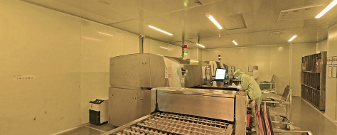
Advanced technology
manufacturing and
production equipment
manufacturing and
production equipment

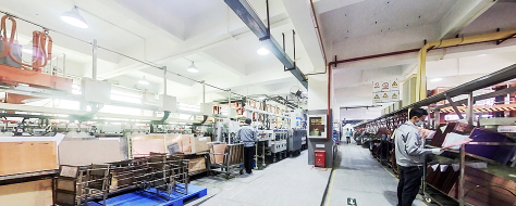
Mature, first-class
fast rotating PCB manufacturing
and assembly
fast rotating PCB manufacturing
and assembly
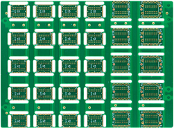
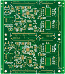
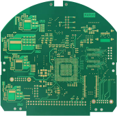
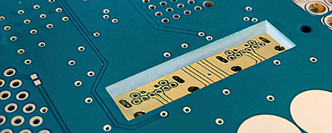
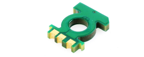
HDI PCB
3rd-order-HDI-PCB-buried-resistor-circuit-board
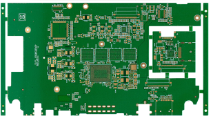
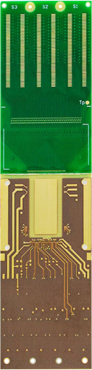
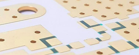
HDI PCB
Ipad-3rd-order-HDI-board
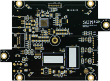
HDI PCB
HDI-second-order-6-layer-immersion-gold
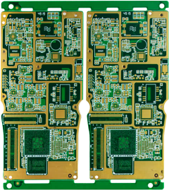
HDI PCB
3rd-order-5G-IoT-HDI-PCB
HDI PCB
Industrial-control-5th-order-HDI-board
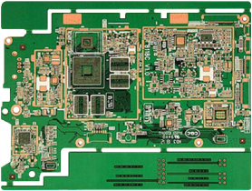
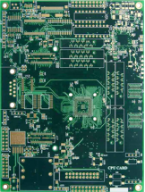
HDI PCB
10-layer-2nd-order-HDI-board
HDI PCB
3rd-order-HDI-board
HDI PCB
Mobile-phone-3rd-order-HDI-board
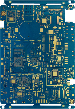
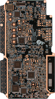
HDI PCB
6th-order-arbitrary-interconnection-HDI-buried
HDI PCB
HDI-second-order-12-layer
HDI PCB
Automotive-communication-2nd-order-HDI-board
HDI PCB
2nd-order-HDI-buried
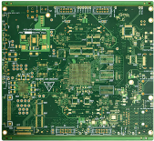
HDI PCB
2nd-order-high-speed-PCB
As printed circuit board technologies increase and electronics continue to get smaller and smaller, you
need to make sure your current circuit board supplier has the appropriate equipment needed for the
specialty processes that are found in more advanced circuit board designs.
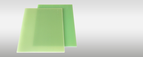
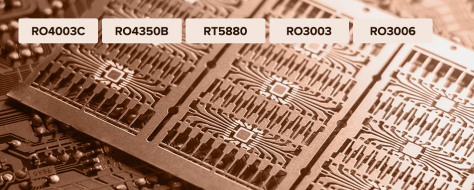
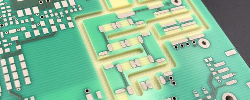
Qualified Materials
- FR-4 Board
- Aluminum Board
- Copper Base
- Rogers
-
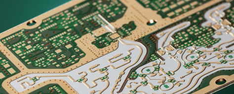
HDI
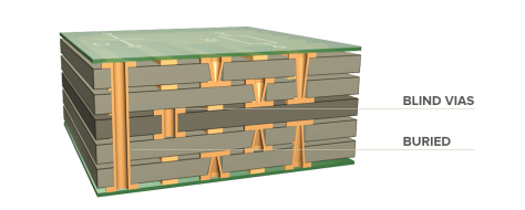
Buried/
blind vias
.png)
.png)
- Immersion gold(ENIG)
- Hard Gold
- ENEPIG
- OSP
- Immersion silver(Ag)
-
HASL
with lead/
lead free - Surface Finish
- Half-cut/ Castellated Holes
- Impedance control
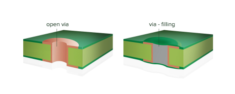
- Buried/ blind vias
- Via filled with resin
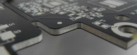
- Countersinks/ Counterbores
- Z-axis milling
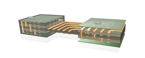
- Custom Stackup
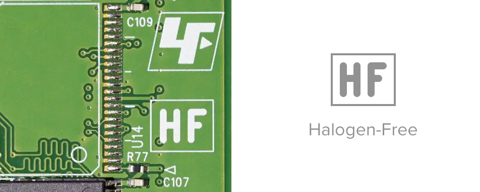
- Halogen-Free
- Additional Options
PCBGOGO PCB Capabilities
|
|
|
|
|
|
|
|
|
|
|
|
|
|
|
|
|
|
|
|
|
|
|
|
|
|
|
|
|
|
|
|
|
|
|
|
|
|
|
|
|
|
|
|
|