
 日本語
日本語
 한국어
한국어

How to Convert Schematic to Gerber Files for PCB Manufacturing?
Every PCB order begins with two very different documents. One describes what your circuit should do. The other tells a machine exactly where to drill, plate, and mask copper. Getting from the first to the second — from schematic to Gerbers — is the workflow that decides whether your design lands on the factory floor or bounces back for revisions.
This guide walks through the entire path: what a schematic actually represents, what a Gerber file contains, how to move cleanly from circuit diagram to physical layout, and how to export, verify, and submit manufacturing-ready files. Along the way, we'll flag the mistakes that most often turn a promising design into a rejected order.
What Is a Schematic?
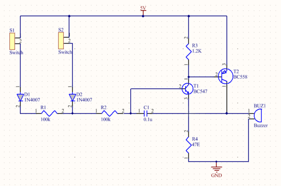
A schematic is a symbolic diagram of an electronic circuit. It shows how components such as resistors, capacitors, ICs, and connectors are electrically connected through signals, or "nets" — but it says nothing about where those parts will physically sit on a board.
Think of it as the logic behind the design. A schematic drives three outputs that everything downstream depends on:
Netlist — defines exactly how every component pin connects to every other pin.
BOM (Bill of Materials) — lists every part, value, and quantity needed to build the circuit.
Reference designators — labels like R1, C5, and U2 that tie the schematic to the layout and, later, to assembly.
A schematic is also where naming discipline pays off. Consistent net names (VCC_3V3, GND, SPI_CLK) and clear power/ground symbols make the design far easier to route, review, and debug later.
What Is a Gerber File?
A Gerber file is a vector image file, based on the RS-274X format, that describes one physical layer of a PCB — copper, solder mask, silkscreen, or drill data. Manufacturing equipment reads these files directly to plate copper, apply mask, print legends, and drill holes.
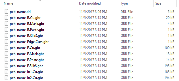
Unlike a schematic, which is usually a single project file, a finished Gerber package is a set of files — one per layer, plus a separate drill file. A typical set includes:
Top and bottom copper layers
Top and bottom solder mask
Top and bottom silkscreen
Top and bottom solder paste (for assembly)
Drill file, in Excellon format
Board outline / mechanical layer
Here's how the two file types compare side by side:
| Aspect | Schematic | Gerber Files |
|---|---|---|
| Purpose | Electrical logic and connections | Physical fabrication instructions |
| Information conveyed | Component connections, nets | Copper shapes, drill holes, layer outlines |
| File count | Typically one project file | One file per layer, plus a drill file |
| Format | EDA-native (.sch, .kicad_sch, etc.) | RS-274X (layers), Excellon (drills) |
| Used by | Circuit designer, reviewer | CAM engineer, fabrication equipment |
Drawing the Schematic: A Quick Overview
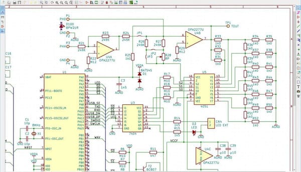
Before any Gerber file exists, the schematic needs to be complete and clean. This isn't the main focus of this guide, but here's the process in brief:
1. Define circuit requirements — target voltage, current, and the functional blocks the design needs (power, MCU, sensors, interfaces).
2. Choose a schematic capture tool that fits your project's complexity and budget.
3. Place components and assign reference designators (R1, C1, U1) as you go.
4. Wire the nets with clear, consistent labels (VCC_3V3, GND, SPI_CLK) rather than default auto-generated names.
5. Run an Electrical Rule Check (ERC) to catch unconnected pins, conflicting outputs, and missing power nets.
6. Generate the BOM and netlist to hand off to PCB layout.
If you haven't settled on a schematic capture tool yet, our guide to the top PCB design software compares KiCad, Altium, Fusion 360, and other popular options so you can pick one that matches your project and skill level.
From Schematic to PCB Layout
Once your schematic passes ERC, the netlist moves into your layout tool, where every pad and pin gets a physical home. This is the stage where logical connections become copper geometry.
A few things matter most during this transition:
Import the netlist rather than re-entering connections manually — this keeps schematic and layout in sync.
Group related components (a microcontroller and its decoupling capacitors, for example) close together to keep traces short.
Route high-speed or high-current nets first, and keep a solid ground plane underneath them for a clean return path.
Re-run design rule checks (DRC) for clearance, trace width, and via specifications before moving on.
If you rename a component or change a connection at this stage, update the schematic first — a mismatch between schematic and layout is one of the most common causes of manufacturing errors. Once your layout passes DRC, it's time to translate the file into the language every fabricator reads: Gerbers.
Exporting Gerber Files and Verifying with a Gerber Viewer
Step 1. Exporting the Files
The exact menu differs by software, but the export process follows the same general pattern in KiCad, Altium, Eagle, and most other tools:
1. Open your finished, DRC-clean layout.
2. Go to the plot/export menu and select Gerber (RS-274X) as the output format.
3. Select every layer you need — copper, mask, silkscreen, paste (if you need assembly), and board outline.
4. Generate a separate drill file in Excellon format for through-holes and vias.
5. Save everything to a single, clearly labeled output folder.
Step 2. Verifying with a Gerber Viewer
Exporting files doesn't guarantee they're correct — a missing layer, a misaligned drill hit, or the wrong units can slip through unnoticed until the files reach the fabricator. Opening the exported set in a Gerber viewer before submission catches these issues while they're still easy to fix.
On this website, you don't need to install separate software to do this. PCBgogo's browser-based Gerber Viewer lets you drag and drop your zipped Gerber and drill files directly and inspect every layer on the spot — no download required.
While reviewing your files in a viewer, check for:
Correct alignment between copper, mask, and silkscreen layers
An accurate board outline and overall dimensions
Drill holes landing where pads and vias expect them
Legible silkscreen text that doesn't overlap pads
No stray or orphaned copper left over from editing
Submitting Gerber Files for Manufacturing
A complete submission avoids back-and-forth with your fabricator's engineering team. At minimum, your file package should include:
| File | Typical Extension | Purpose |
|---|---|---|
| Top / Bottom Copper | .GTL /.GBL | Conductive trace layers |
| Top / Bottom Solder Mask | .GTS /.GBS | Solder mask openings |
| Top / Bottom Silkscreen | .GTO /.GBO | Component labels and markings |
| Drill File (Excellon) | .TXT /.DRL | Hole locations and sizes |
| Board Outline | .GKO /.GML | Board shape and dimensions |
| Top / Bottom Paste | .GTP /.GBP | Stencil apertures, needed for SMT assembly |
| Fabrication Notes (optional) | .TXT / .PDF | Stack-up details, special instructions |
Package the full set into a single ZIP file with clear, consistent naming, and double-check that nothing was left out of the export. If your board has special requirements — an unusual stack-up, a non-standard surface finish, or specific silkscreen colors — a short readme note included with the files helps the fabrication team get it right the first time.
PCBgogo's Capabilities: PCBgogo has been manufacturing PCBs since 2013 and holds ISO 9001:2015 and UL certification. Beyond standard fabrication, the team supports HDI fabrication, X-ray inspection for BGA and other hidden joints, DFM checking to catch design issues before production, and precision SMT assembly for turnkey builds — with a 1-board minimum order that makes it practical to prototype a schematic-to-Gerber workflow without committing to a large production run.
Common Mistakes to Avoid
At the Schematic Stage
Missing or duplicate reference designators that cause confusion later in layout and assembly
Unclear or inconsistent net names, especially on power rails
Skipping the ERC step before handing the design off to layout
At the Layout Stage
Ignoring DRC clearance violations without reviewing and resolving them.
Forgetting a solid ground plane or return path for high-speed signals
Footprints that don't match the schematic's component or pin count
At the Export Stage
Forgetting to generate or include the drill file
Exporting in an outdated or non-standard Gerber format your fabricator can't read
Mismatched units (mm vs. inch) between layers
Sending an incomplete file set — missing a layer or the board outline
Skipping the Gerber viewer check before submission
FAQ
What is the difference between a schematic and a Gerber file?
A schematic shows the electrical logic of a circuit — how components connect. A Gerber file describes the physical layers of the finished board — copper shapes, drill holes, and outlines — in a format manufacturing equipment can read directly.
How do I convert a schematic into Gerber files?
Finish the PCB layout using the schematic's netlist, run a design rule check, then export each layer (copper, mask, silkscreen) as RS-274X Gerber files along with an Excellon drill file from your EDA software's plot or export menu.
What files do I need besides Gerber files when submitting for manufacturing?
At minimum, include a drill file and a board outline layer. For assembly, also include a BOM, pick-and-place file, and paste layers. A short fabrication notes file helps communicate any special requirements.
Do I need special software to check Gerber files before ordering?
No. A Gerber viewer is enough, and browser-based options like PCBgogo's Gerber Viewer let you check layer alignment, drill placement, and board outline without installing anything.
What's the difference between RS-274X and Excellon file formats?
RS-274X is the standard format for Gerber layer files — copper, mask, and silkscreen. Excellon is a separate format used specifically for drill files, describing hole locations, sizes, and plating information.





