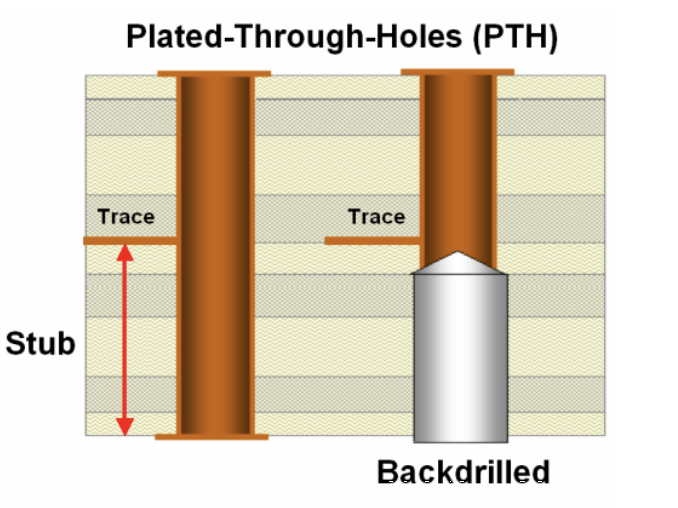
Back drilling, or controlled depth drilling, is a process used on high-speed multi-layered PCBs to remove the stubs from plated through-holes or vias. The stubs are the unwanted portions of the vias. Back drilling can be applied to any PCB types. We know that drilling is a time-consuming and expensive process in PCB manufacturing. And it is also a process that has certain challenges to technology, and the back drilling process is the same.

____________________________________________________________________________________________________________________________
Why need back drilling in PCB manufacturing?
The stubs are the source of signal reflections and impedance discontinuities. And the signal integrity will also be affected by the stubs. Back drilling may be the ideal solution if the PCBs are suffering from a high bit error rate (BER), deterministic jitter, signal attenuation, or other EMI problems. The signal distortion will be severe if the stub is long.
Why we use back drilling rather than blind vias or buried vias to manage the signal quality for high-speed signal applications? Because back drilling cost is lower compared to the technologies of blind and buried vias. And using back drilling can also greatly reduce the difficulty of PCB manufacturing.
____________________________________________________________________________________________________________________________
What is the process of back drilling?
Usually, back drilling is the final step of PCB manufacturing. The procedure of back drilling is as below:
Material cutting ? Inner layer process ? Etching ? AOI ? Oxide ? Pressing ? Drilling ? PTH ? Outer layer process ? Inspection ? Pattern plating ? Back drilling
The drilling machines are computer-controlled. The correct program the operator chooses will tell the machine the X-Y ordinate of the holes and which drill to use. And the drill used for back drilling is slightly larger than the vias to remove the conductive coating or stubs from the hole. There are usually two kinds of drilling technologies; laser drilling and mechanical drilling. Laser drilling is more precise, and mechanical drilling is easier to operate. Back drilling usually uses mechanical drilling technology.
There are some manufacturing points we should pay more attention to back drilling. Firstly, we would better use new drill tools to reduce chip load. Secondly, PCB manufacturers should check all the factors that may affect the precise of back drilling to improve the capability of back drilling. Thirdly, using suitable back drilling methods and advanced equipment to best control the depth accuracy of back drilling.
____________________________________________________________________________________________________________________________
The back-drilling capability of PCBGOGO
The minimum diameter of a back drilling hole is 0.3mm. The board thickness should be over 2.5mm. And the tolerance of back drilling depth is +/- 0.05mm.
Drilling is the most critical and difficult process because even a small error can cause a great loss. You should consider the capabilities of the PCB manufacturers before placing orders. PCBGOGO is specialized in PCB prototype assembly and providing back drill board with competitive prices. High reliability and short lead-time are our advantages. If you have any idea about PCB prototype or PCB assembly, please contact our online services or send Emails to us.
