


A practical guide to stencil types, selection criteria, production files and custom manufacturing options.
Solder paste printing may look like a simple step, but it has a major influence on PCB assembly quality. Too much paste can cause solder bridging, while too little may result in weak or incomplete joints. An accurately made SMT stencil helps control this process by depositing the right amount of solder paste on each PCB pad.
However, not every stencil suits every project. Production volume, component size, printing equipment and PCB layout all need to be considered. This guide explains the differences between framed and frameless SMT stencils and how to select the right option.
An SMT stencil, also called a PCB stencil or solder paste stencil, is a thin sheet - usually made of stainless steel - with precisely cut apertures that match the surface-mount pads on a PCB.
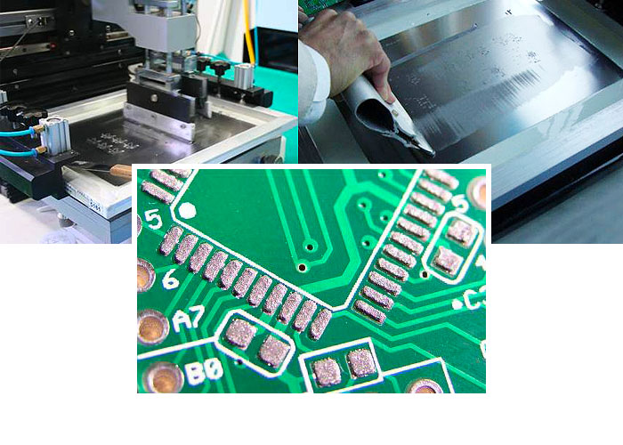
During printing, the stencil is aligned over the bare circuit board. A squeegee pushes solder paste across its surface and through the apertures. When the stencil is lifted, controlled deposits of paste remain on the pads, ready for component placement and reflow soldering.
The stencil pattern is normally created from the top or bottom solder paste layer in the PCB Gerber files. The PCB outline and fiducial information may also be required for correct positioning. For a complete PCBA order, manufacturers usually need additional files such as the BOM and pick-and-place file, but the paste layer is the main PCB file used to produce the stencil.
Squeegee solder paste through the stencil; the stencil ensures the solder paste is the right amount in the right position. Then you can place surface mount components on the solder paste and put it into a reflow oven.
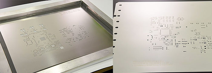
The two most common options are framed and frameless SMT stencils. Both perform the same basic function, but their structures and intended applications are different.
A framed stencil consists of a laser-cut metal foil permanently stretched inside a rigid aluminum frame. The frame keeps the foil flat and under consistent tension, making alignment and solder paste printing more repeatable.
Framed stencils are generally preferred for automated or semi-automated printing, repeated assembly runs and medium- to high-volume production. Their stability reduces stencil movement and makes them easier to use over many printing cycles.
The main disadvantages are their higher cost, larger storage footprint and greater shipping weight.
A frameless stencil is a laser-cut metal sheet without a permanently attached frame. It can be placed directly over the PCB for manual printing or mounted in a reusable tensioning system.
Because it is compact and lightweight, a frameless SMT stencil is well suited to prototypes, DIY assembly and low-volume production. It is also easier to customize around a small PCB, helping reduce unnecessary material and shipping costs.
Manual alignment requires more care, however, and an unsupported foil may not provide the same printing consistency as a permanently framed stencil during long production runs.
Selecting a stencil involves more than choosing between a frame and a bare sheet. The following factors directly affect printing performance.
For a few prototype boards, a frameless stencil is often the most economical choice. If the same PCB will be assembled repeatedly, a framed stencil provides better tension, faster alignment and more consistent results.
Stencil size and printable area are not the same. The board data must fit inside the valid cutting area, with sufficient space around the PCB for alignment and squeegee movement.
A very large stencil may be unnecessary for a small board. A custom-size frameless stencil can save material, storage space and shipping cost. For automated printing, confirm that the frame dimensions are compatible with the machine.
Stencil thickness controls solder paste volume. Fine-pitch ICs, small passive components and dense BGA layouts generally benefit from thinner foil and carefully optimized apertures. Larger pads, power components and connectors may require a greater paste volume.
Common thicknesses include 0.10, 0.12 and 0.15 mm, although the best choice depends on the smallest aperture, pad geometry and component mix. Boards containing both fine-pitch devices and large components may require modified apertures or a step stencil.
Stencil apertures do not always need to match PCB pads exactly. Their dimensions can be reduced or reshaped to improve paste release and prevent defects such as bridging, solder balls and tombstoning.
For example, thermal pads under QFN components are often divided into several smaller openings instead of one large aperture. A manufacturing review is recommended when the PCB contains fine-pitch packages, BGAs or unusually large thermal pads.
Fiducials help printing equipment align the stencil with the PCB. Automated machines commonly use partially engraved fiducials, while through-cut fiducials can assist manual or semi-automatic alignment.
Electropolishing removes small burrs and smooths aperture walls, allowing solder paste to release more easily. It is especially useful for fine-pitch ICs and BGA components.
Before ordering, provide the appropriate top and/or bottom solder paste Gerber layer. Clearly specify whether the stencil is required for one side or both sides of the PCB.
It is also helpful to include:
Accurate and clearly named PCB files reduce engineering questions and help prevent stencil revisions.
PCB outline dimensions
Fiducial requirements
Stencil thickness
Framed or frameless construction
Required stencil dimensions
Any special aperture instructions
PCBgogo provides laser-cut framed and frameless SMT stencil manufacturing for PCB prototypes, small batches and production assembly. Customers can choose from multiple stencil sizes and request custom dimensions based on their PCB layout and printing process.
Available order options include 0.10, 0.12, 0.15 and 0.20 mm thicknesses, top or bottom-side configurations, fiducial treatments and electropolishing. If the PCB was previously ordered through PCBgogo, the existing PCB file can also be selected for stencil production, simplifying file submission.
By ordering the PCB and stencil from the same manufacturer, engineers can reduce the risk of mismatched revisions and ensure that the stencil apertures correspond to the final production data.
Next step: Review PCBgogo's SMT stencil quotation options for framed, frameless and custom-size requirements.
A well-designed SMT stencil improves solder paste consistency, reduces assembly defects and makes component placement more reliable. Frameless stencils are practical for prototypes and manual printing, while framed stencils offer the stability required for repeated or automated production.
Before ordering, review the printable area, thickness, aperture design, fiducials and PCB paste layers. Matching these parameters to the board design and production process will deliver better results than selecting a stencil based on price alone.
It is strongly recommended for boards containing surface-mount components. A stencil applies solder paste faster and more consistently than dispensing paste onto individual pads by hand.
The main file is the top or bottom solder paste layer from the PCB Gerber package. The PCB outline and fiducial data may also be needed for sizing and alignment.
Choose a frameless stencil for prototypes, small batches and manual printing. A framed stencil is generally better for automated equipment, repeated printing and higher production volumes.
The correct thickness depends on pad dimensions and component types. Fine-pitch components usually require thinner foil, while larger pads may need more solder paste. Ask the manufacturer to review mixed-component layouts.
Yes. Top and bottom patterns may sometimes be placed on one sheet if there is enough usable area and manual printing is planned. Separate stencils are usually more convenient for automated production.

 日本語
日本語
 한국어
한국어

