



What sets a high-performance PCB apart often comes down to details you can barely see: finer traces, smaller vias, more complex stackups, and tighter control over impedance, copper thickness, and dimensions. As automotive electronics, industrial systems, communications equipment, and consumer devices become faster, denser, and more compact, standard PCB manufacturing is not always enough. PCBgogo combines advanced processes with rigorous quality control to turn complex designs into reliable, production-ready boards. Read on to explore our advanced PCB manufacturing capabilities and see how we support even the most demanding projects.
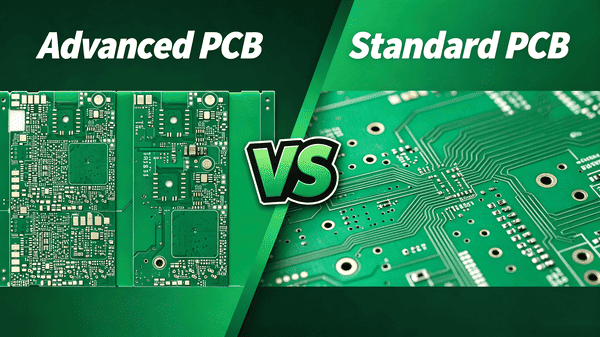
The difference is not simply the number of layers. It comes down to design complexity, performance requirements, and manufacturing precision.
Standard PCBs use established structures and common production requirements. They are a practical, cost-effective choice for straightforward electronic designs.
Advanced PCBs are built for applications with tighter space, higher signal demands, challenging operating conditions, or strict reliability requirements.
The manufacturing process also becomes more demanding. Advanced designs require closer engineering review, tighter process control, and more extensive inspection and testing.
Producing these boards reliably takes more than standard equipment. It requires strong engineering support and proven manufacturing expertise. These are exactly the strengths PCBgogo brings to every advanced PCB project. Below, we take a closer look at PCBgogo's advanced PCB capabilities.
| PCB technology | Key manufacturing capability | Typical materials | Common applications |
|---|---|---|---|
| HDI PCB | Microvias down to 0.10 mm for production and 0.075 mm for engineering-reviewed prototypes; sequential lamination, stacked/staggered microvias and via-in-pad | High-Tg FR-4, halogen-free FR-4, RCC, low-Dk prepreg | Smartphones, wearables, medical devices, compact industrial electronics |
| High-frequency and RF PCB | Pure RF and hybrid constructions; 3/3 mil trace/space at 1 oz on qualified constructions; controlled impedance | Rogers RO4003C/RO4350B/RO5880, PTFE, Taconic, low-loss materials | 5G, antennas, radar, RF modules, microwave systems |
| High-speed digital PCB | Low-loss materials, back drilling, impedance control and multilayer stack-up engineering | Megtron 6/7, Isola I-Tera MT40, FR408HR and equivalent qualified materials | AI servers, data centers, networking and high-speed computing |
| High-layer-count PCB | Up to 40 layers; blind/buried vias, back drilling, resin-filled vias and custom stack-ups | FR-4, high-Tg, halogen-free and low-loss laminates | Servers, telecom, industrial control, medical and automotive electronics |
| Flexible PCB | Up to 12 layers on engineering-reviewed builds; fine lines, laser vias, coverlay, stiffeners and EMI shielding options | Polyimide, RA/ED copper, PET where applicable | Cameras, displays, wearables, sensors and compact interconnects |
| Rigid-flex PCB | Rigid and flexible sections in one multilayer structure; HDI and controlled impedance available by review | Polyimide flex materials combined with FR-4 | Medical, aerospace, automotive, robotics and compact assemblies |
| Metal-core and thermally enhanced PCB | Aluminum, copper, embedded-metal and thermoelectric-separation structures | Aluminum, copper, thermally conductive dielectric systems | Power electronics, LED, EV, charging and industrial power systems |
| Ceramic substrate | Al2O3, AlN and Si3N4 options; DBC, DPC, HTCC and LTCC processes according to design | Alumina, aluminum nitride, silicon nitride | Power modules, optoelectronics, RF, automotive and high-temperature electronics |
| Manufacturing Item | Prototype Limit | Small/Medium-Volume Limit | Design Note |
|---|---|---|---|
| Rigid PCB layer count | 1-40 layers | 1-32 layers | Stack-up and material review required |
| Finished board thickness | 0.2-7.0 mm | 0.45-6.0 mm | Hole aspect ratio and warpage requirements apply |
| Minimum size | 2*2 mm | 5*5 mm | Panelization and handling method must be confirmed |
| Maximum size | ≤2 layers: 660*1143 mm; | ≤2 layers: 660*1143 mm ≥3 layers: 648*965 mm | Subject to material and working-panel utilization |
| Minimum finished mechanical hole | 0.125 mm | 0.125 mm | Corresponding minimum tool is 0.15 mm; practical limit depends on thickness |
| Minimum laser microvia | 0.075 mm | 0.10 mm | Maximum depth-to-diameter ratio: 1.2:1 prototype; 1:1 volume |
| Maximum PTH aspect ratio | 20:1 with drill >0.20 mm | 12:1 with drill >0.20 mm; 10:1 with 0.20 mm drill | Material and plating reliability apply |
| Resin-filled finished hole | 0.10-0.90 mm | 0.10-0.90 mm | Corresponding drill range: 0.15-1.00 mm |
| Minimum inner trace/space at 1/3 or 1/2 oz | 2.5/2.5 mil | 3/3 mil | Limits vary depending on copper weight |
| Minimum inner trace/space at 1 oz | 3/4 mil | 3/4 mil | — |
| Minimum outer trace/space at 1/3 oz | 3/3 mil | 3.5/4 mil | — |
| Minimum outer trace/space at 1/2 oz | 3.5/3.5 mil | 3.5/4 mil | — |
| Minimum outer trace/space at 1 oz | 3.5/3.5 mil | 4/4 mil | — |
| Maximum finished copper | Inner 8 oz; outer 8 oz | Inner 4 oz; outer 6 oz | Feature limits become wider as copper increases |
| Controlled impedance | Single-ended/differential: ±5 Ω at ≤50 Ω; ±10% above 50 Ω; ±5% extreme by review | ±5 Ω below 50 Ω; ±10% at ≥50 Ω | TDR coupon and stack-up data may be required |
| Minimum controlled-depth back-drill depth | 0.10 mm | 0.10 mm | Back-drill depth tolerance: ±0.075 mm |
| Minimum insulating layer | 2 mil | 2 mil | Limited to qualified low-copper constructions |
| Surface finishes | ENIG, ENEPIG, OSP, immersion tin, immersion silver, HASL/lead-free HASL, hard gold, soft gold and selected mixed finishes | Same | Finish availability depends on material, copper and assembly requirements |
The figures above are process boundaries, not universal design rules. For the best balance of yield, reliability, price and lead time, design away from the minimum whenever routing density allows.
PCBgogo - Reliable, High-Quality PCB Manufacturing
Save time and money with an all-in-one solution for PCB fabrication, assembly, and parts. Reduce vendor coordination, avoid split shipments, and get consistent, reliable quality.
Get Free Quote >
HDI technology increases routing density through laser-drilled microvias, finer conductors, smaller pads and sequential lamination. PCBgogo supports common 1+N+1, 2+N+2 and 3+N+3 constructions, as well as more complex stacked-via and any-layer concepts subject to engineering approval. Available processes include copper-filled laser vias, resin-filled via-in-pad, staggered and stacked microvias, blind and buried vias, and sequential lamination.
| Parameter | Small/Medium-Volume Capability | Prototype Capability |
|---|---|---|
| Layer count | 4-16 layers | 4-24 layers |
| Finished board thickness | 0.6-3.2 mm | 0.4-6.0 mm |
| HDI structure | Up to 4+N+4 by engineering review | Any-layer interconnect by engineering review |
| Minimum laser microvia | 4 mil/0.10 mm | 3 mil/0.075 mm |
| Minimum trace/space | 2.5/2.5 mil | 2.5/2.5 mil |
| Minimum finished through-hole | 8 mil/0.20 mm | 6 mil/0.15 mm |
| Minimum dielectric thickness | 3 mil | 2 mil |
| Minimum pad size | 12 mil | 10 mil |
| Microvia depth-to-diameter ratio | 1:1 | Up to 1.2:1 |
| Layer-to-layer registration | ±3 mil | ±2 mil |
| Solder mask registration | ±2 mil | ±1 mil |
| Impedance tolerance | ±10% | Up to ±7% by review |
| Microvia copper | 12-18 μm | 12-18 μm |
For stacked microvias, via-in-pad, multiple sequential laminations or high-current designs, send the proposed stack-up together with the fabrication data. We evaluate microvia geometry, dielectric thickness, copper distribution and reliability requirements as one system rather than approving each parameter independently.
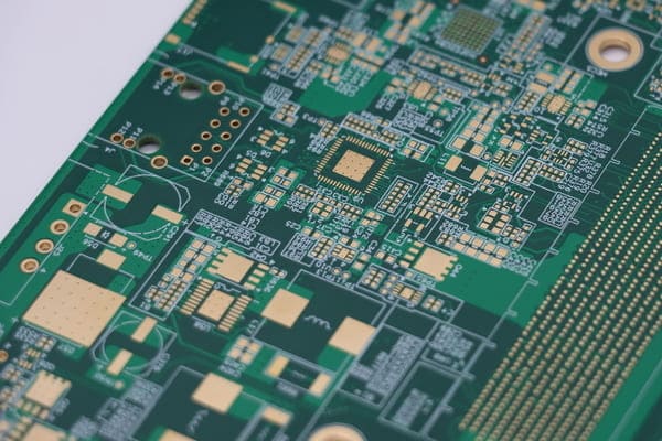
High-frequency and high-speed boards require more than a low-loss laminate. Material Dk/Df, copper profile, dielectric thickness, conductor geometry, surface finish, registration and impedance all influence signal performance. PCBgogo supports pure RF laminate builds and hybrid constructions that combine RF materials with FR-4 or other qualified laminates.
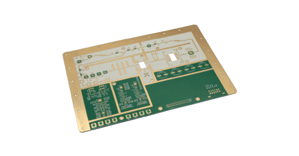
| Parameter | Pure/Hybrid RF Construction | PTFE Reference Construction |
|---|---|---|
| Layer count | 4–16 layers | Project-specific |
| Minimum trace/space | 3/3 mil at 1 oz | 6/6 mil at 1 oz |
| Finished board thickness | 0.8-3.2 mm | 0.508 mm reference build; other thicknesses by review |
| Minimum CNC finished hole | 0.15 mm | 0.20 mm |
| CNC hole aspect ratio | Up to 12:1 | Stack-up dependent |
| Laser microvia | 0.075-0.15 mm | Material and construction dependent |
| Microvia aspect ratio | Up to 1:1 | Material and construction dependent |
| Minimum PTFE pad | — | 0.25*0.25 mm |
| Construction options | Pure RF lamination, hybrid lamination, blind/buried vias, via-in-pad, back drilling | PTFE processing, plated through-holes and controlled impedance |
| Surface finishes | ENIG, ENEPIG, immersion silver, immersion tin, OSP, HASL/lead-free HASL and hard gold | Selected according to RF and assembly requirements |
| Material Family | Reference Dk at 10 GHz | Reference Df at 10 GHz | Typical Use |
|---|---|---|---|
| Rogers RO4350B | 3.48 | 0.0037 | 5G, RF modules and base-station equipment |
| Rogers RO4003C | 3.55 | 0.0027 | Cost-effective RF and high-frequency signal transmission |
| Rogers RO5880 | 2.20 | 0.0009 | Radar, aerospace and millimeter-wave circuits |
| PTFE material families | 2.1-2.6 | 0.0002-0.001 | Very-low-loss microwave and RF designs |
| Panasonic Megtron 6/7 | 3.3-3.5 | 0.002-0.003 | Data centers and high-speed interconnects |
| Isola I-Tera MT40 | 3.45 | 0.0028 | 28 Gbps+ high-speed systems |
| Taconic T-35/TLX families | 3.2-3.5 | 0.0018-0.003 | RF communications and thermally stable designs |
| Isola FR408HR | 3.66 | 0.008 | Cost-sensitive mid- to high-speed designs |
Material values are references for initial selection, not stack-up calculation inputs. Always confirm the exact laminate grade, test method, resin content, thickness and manufacturer data sheet for the production lot.
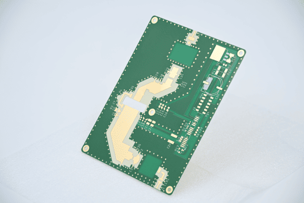
High-layer-count PCBs create additional challenges in registration, lamination, drilling, copper plating, impedance consistency and warpage control. PCBgogo provides stack-up, back-drill, impedance and panelization review for complex multilayer designs used in high-speed computing, networking, telecommunications, medical and industrial systems.
| Parameter | Capability |
|---|---|
| Maximum layer count | 40 layers |
| Minimum trace/space | 3/3 mil |
| Minimum CNC finished hole | 0.15 mm |
| Finished board thickness | 0.8-6.0 mm |
| Standard board-thickness tolerance | ±10% |
| Material systems | FR-4, high-Tg, halogen-free and high-frequency/low-loss materials |
| Interconnect options | Through-hole, blind/buried vias, HDI and any-layer structures by review |
| Signal-integrity options | Controlled impedance, back drilling, low-loss materials and custom stack-ups |
| Surface finishes | ENIG, ENEPIG, immersion silver, OSP, nickel/gold and other qualified finishes |
| Process control | LDI, AOI, automated electrical test, four-wire low-resistance test and microsection analysis as required |
For boards approaching maximum layer count or thickness, include the target stack-up, finished copper by layer, impedance table and back-drill requirements with the RFQ.
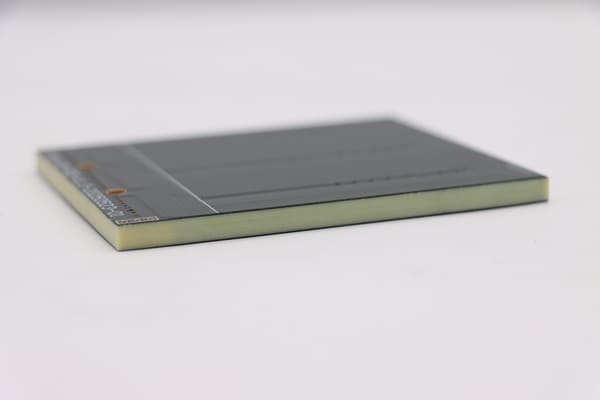
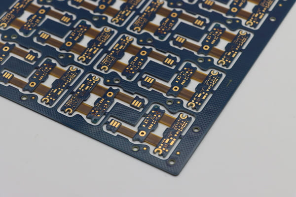
Flexible and rigid-flex PCBs reduce connector count, save space and support three-dimensional packaging. Their manufacturability depends on the relationship between flex thickness, copper type, bend direction, bend radius, coverlay openings, stiffeners and the rigid-to-flex transition—not only on layer count and line width.
PCBgogo's Flexible PCB Capabilities cover builds up to 12 layers, with fine-line routing, laser vias, coverlay, stiffeners and EMI shielding options suited to cameras, displays, wearables and compact interconnects.
Our Rigid-Flex PCB Capabilities extend to structures that combine rigid and flexible sections in one build, supporting up to 16 total layers, with HDI, laser vias and controlled impedance available by engineering review—commonly used in medical, aerospace, automotive and robotics assemblies.
Dynamic-flex designs require the bend radius, flex cycles, bend direction and installed geometry. We recommend rolled-annealed copper and a dedicated dynamic-flex review where repeated movement is expected.
Metal-core and embedded-metal constructions move heat away from power devices and improve mechanical stability. PCBgogo supports aluminum, copper, cold-plate, sintered and embedded-metal structures for lighting, power conversion, EV, industrial control and high-current applications.
Our Aluminum PCB Capabilities and Copper PCB Capabilities each cover the full build range for their respective metal-core constructions, including layer count, board thickness, copper weight and surface finishes.
Ceramic substrates combine electrical insulation with thermal conductivity, dimensional stability and high-temperature performance. PCBgogo supports alumina, aluminum nitride and silicon nitride options for power modules, LEDs, optoelectronics, RF circuits, sensors and automotive electronics.
| Parameter | Capability |
|---|---|
| Layer count | 1-2 layers |
| Ceramic materials | Al2O3, AlN and Si3N4 |
| Process options | DBC, DPC, HTCC and LTCC according to design |
| Finished size | 5*5 mm to 100*100 mm for small/medium volume; up to 140*140 mm for reviewed prototypes |
| Standard finished board thickness | 0.38-2.0 mm |
| Ceramic dielectric options | 0.20, 0.25, 0.30, 0.381, 0.50, 0.635, 0.80, 1.00, 1.20 and 1.50 mm by material/process review |
| Minimum trace/space | 4/4 mil with ±0.05 mm line tolerance on qualified processes |
| Minimum laser hole | 0.20 mm |
| Copper weight | 0.5-3.0 oz; local thickening by review |
| Reference thermal conductivity | 24-28 W/m·K for Al2O3; 170-200 W/m·K for AlN; 80-90 W/m·K for Si3N4 |
| Surface finishes | ENIG, ENEPIG, immersion silver, immersion tin and OSP according to process |
Choose Al2O3 when cost and general thermal performance are the priority, AlN for high heat flux, and Si3N4 when mechanical strength, crack resistance and vibration performance are central to the design.
| Material Category | Prototype Options | Small/Medium-Volume Options |
|---|---|---|
| HDI dielectric systems | RCC 65T/100T; LDPP IT-180A 1037/1086; standard PP 106/1080 | Same qualified systems |
| High-Tg halogen-free FR-4 | Shengyi S1165; Kingboard HF-170 | Shengyi S1165; Kingboard HF-170 |
| General-Tg halogen-free FR-4 | Shengyi S1155; Kingboard KB-6165G | Shengyi S1155; Kingboard KB-6165G |
| High-CTI | Shengyi S1600L; Kingboard KB6165GC/KB-6169GT | Same qualified systems |
| High-Tg FR-4 | FR408/FR408HR, IS410, FR406, GETEK, PCL-370HR, S1000-2, IT180A, N4000-13 families, Megtron 4/6 and other qualified grades | IT180A, GETEK, PCL-370HR, N4000-13 families, S1000-2/S1000-2M |
| Ceramic-filled RF | Rogers RO4350B/RO4003/RO4725/RO4730; Shengyi SJ9033/SJ9036 | Rogers RO4350B/RO4003; Shengyi SJ9033/SJ9036 |
| Ceramic-filled bondply | RO4450T/F; SJ930B/SJ936B | RO4450F; SJ930B/SJ936B |
| PTFE high-frequency | Rogers/Arlon and Taconic families; F4BM/TP and other qualified suppliers | Taconic TLX/TLF/TLY/RF/TLC/TSM; Rogers/Arlon RO3/RO5, Diclad, AD and CLTE families; F4BM and qualified Shengyi options |
| PTFE bondply | Rogers 6700; Taconic FR-28; RT6002 | Rogers 6700; Taconic FR-28 |
| Hybrid lamination | Rogers/Arlon, Taconic, Nelco or Shengyi SJ combined with FR-4, including local RO4350 hybrid lamination | Rogers/Arlon, Taconic or Shengyi SJ combined with FR-4, including local RO4350 hybrid lamination |
| General FR-4 | Shengyi S1141/S1000H; ITEQ IT158; Kingboard KB-6160/KB-6165 | Same qualified systems |
Material availability can vary by laminate thickness, copper type and production quantity. If an exact manufacturer and material code are mandatory, state "no substitution" in the fabrication notes.
| Process | What It Supports |
|---|---|
| Sequential lamination | Multi-stage HDI, buried vias and complex interconnect structures |
| Laser drilling | Microvias and high-density interconnection |
| Copper-filled microvias | Stacked microvias and via-in-pad routing |
| Vacuum resin filling | Planar via-in-pad, BGA/QFN assembly and improved soldering reliability |
| Back drilling | Reduced via stubs for high-speed and high-frequency channels |
| Controlled-depth drilling/milling | Blind mechanical holes, cavities and stepped PCB structures |
| Controlled impedance | Single-ended and differential transmission lines with TDR verification as specified |
| LDI and AOI | Fine-line imaging, registration control and automated defect detection |
| ENIG | Flat solderable surface for fine-pitch SMT and BGA assembly |
| ENEPIG | Soldering and wire-bonding compatibility with strong corrosion resistance |
| Immersion silver | Flat surface and low signal loss for high-frequency applications |
| Hard gold | Wear-resistant contacts, edge connectors and gold fingers |
| OSP | Flat, lead-free and cost-effective copper protection |
Stack-up, material availability and substitution rules
Minimum conductors, clearances, pad sizes and annular rings
Microvia type, via depth, aspect ratio and sequential lamination count
Copper balance, finished copper and plating requirements
Controlled-impedance geometry, reference planes and test coupons
Back-drill layers and permitted residual stub
Flex bend areas, coverlay, stiffeners and rigid-to-flex transitions
Thermal path, metal base and ceramic material selection
Panelization, tooling, assembly rails and dimensional tolerances
Inspection and verification can include incoming material inspection, online AOI, electrical testing, four-wire low-resistance testing, TDR impedance testing, X-ray inspection, microsection analysis and project-specific reliability testing. The referenced production capabilities support ISO 9001, IATF 16949, ISO 13485 and UL quality systems, with IPC-6012 Class 2 and Class 3 requirements available according to project needs. The applicable acceptance class, reports and documentation should be specified for each order.
Turn your advanced PCB design into a reliable, production-ready product—with expert engineering support from prototype to volume manufacturing. Upload your PCB files today for a comprehensive engineering review and quotation. Let us know which requirements are fixed and where alternatives in materials, stack-up, or processes are acceptable. Our engineers will evaluate the complete build and recommend the most practical, cost-effective path to successful validation and repeatable production. Start your project now and manufacture with confidence.
An advanced PCB uses materials, structures or process controls beyond a conventional through-hole FR-4 board. Common examples include HDI, high-frequency, high-speed, high-layer-count, flexible, rigid-flex, heavy-copper, metal-core and ceramic PCBs.
Yes. Available options include blind and buried vias, laser microvias, copper-filled microvias, resin-filled via-in-pad, and stacked or staggered structures. The approved combination depends on the stack-up, via geometry, lamination count and reliability requirements.
The standard production minimum is 0.10 mm. A 0.075 mm microvia may be available for qualified prototype constructions after engineering review.
±10% is the standard capability. Tighter tolerances may be possible depending on the material, trace geometry, layer construction, coupon design and testing plan.
Yes. Hybrid constructions can combine qualified Rogers, PTFE or other RF laminates with FR-4 to balance signal performance, mechanical requirements and cost. The bondply, copper profile, CTE and lamination cycle must be reviewed together.
Yes. PCBgogo provides PCB fabrication, component sourcing and assembly in one coordinated workflow. Assembly requirements such as fine-pitch BGA, X-ray inspection, special thermal profiles and functional testing should be included with the RFQ.

 日本語
日本語
 한국어
한국어

