


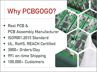
A reliable PCB assembly process is about far more than placing components on a board. Every stage, from reviewing design files and sourcing parts to soldering, inspection, and functional testing, can affect the quality and performance of the finished product. For engineers and product teams, understanding how these steps work together makes it easier to prevent delays, reduce manufacturing risks, and move confidently from prototype to production. In this guide, we'll walk through PCBgogo's PCB assembly process, explain what happens at each stage, and show how careful manufacturing and quality control help turn your design into a dependable, production-ready circuit board.
The PCB assembly process, often called the PCBA process, is the series of operations used to mount and solder electronic components onto a manufactured PCB. A PCB is the bare board containing traces, pads, and vias. It becomes a PCBA after resistors, capacitors, connectors, integrated circuits, and other components have been installed.
Assembly is different from PCB fabrication, although the two are closely connected. Fabrication creates the physical board from Gerber data. Assembly follows by checking files, preparing materials, applying solder paste, placing and soldering components, and inspecting the finished board. The workflow can also include IC programming and functional testing.
Component package, board material, quantity, soldering requirements, and test coverage all affect the production route. A defined process turns these variables into a stable, traceable manufacturing sequence.
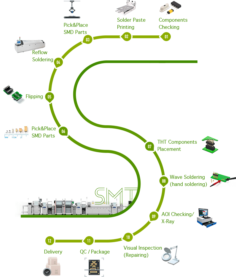
The assembly team reviews the Gerber files, bill of materials, pick-and-place data, and assembly drawings. Part numbers, footprints, polarity, and locations must agree across all files.
A design-for-manufacturing check can identify missing data, unsuitable pads, unclear orientation, or problematic spacing. Resolving these issues early is easier than correcting assembled boards.
Customers can supply their own components or have PCBgogo source the components listed in their approved BOM.. In either case, the components are inspected upon arrival to verify manufacturer part numbers, packages, quantities, values, and physical condition. Bare PCBs are checked at this stage as well, while moisture-sensitive and electrostatic-sensitive components receive appropriate storage and handling throughout the assembly process.
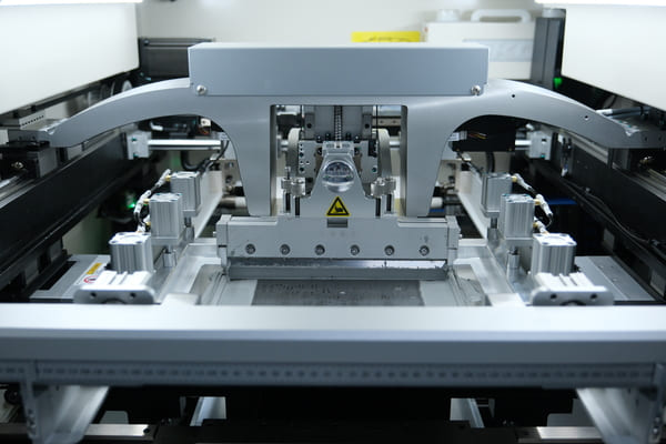
For SMT assembly, a stencil is aligned over the PCB and solder paste is deposited onto the pads. The stencil openings control where the paste is applied and how much is deposited.
Too little paste may create weak or open joints, while excess paste can cause bridging between nearby pads. Stencil design must therefore match the pad layout and fine-pitch component requirements.
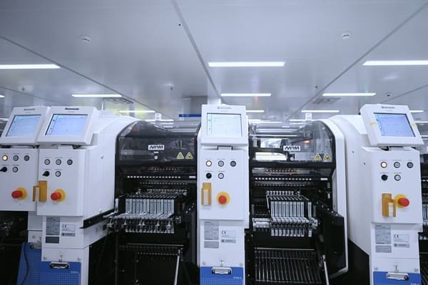
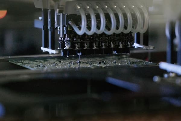
Automated pick-and-place equipment takes components from reels, tubes, or trays and positions them according to the placement file. Machine setup controls the coordinates and rotation of each part, while polarity-sensitive components require particular attention.
Accurate placement is essential for miniature packages and fine-pitch ICs. A placement error at this stage can result in open connections, short circuits, or components that do not function correctly.
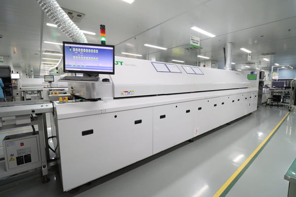
After placement, the board travels through a reflow oven with a controlled thermal profile. During preheating, soaking, reflow, and cooling, the solder paste melts and forms joints between component terminals and PCB pads.
The reflow profile must suit the solder alloy, board construction, component density, and temperature limits of the devices. Proper control helps prevent cold joints, excessive solder voids, component damage, and board warping.
Through-hole parts are normally inserted after the main SMT process. Depending on component type, layout, and quantity, they may be soldered manually or by wave soldering.
Mixed assembly requires careful sequencing so later operations do not disturb mounted components. Parts that cannot tolerate a particular soldering process may need to be installed separately.
Through-hole components are soldered using wave or hand soldering, depending on the board layout, component requirements, and production quantity. Wave soldering may also join compatible, adhesive-secured underside SMDs. Process settings and protective tooling are selected to achieve sound joints while protecting previously assembled parts.
Boards are checked for missing or misplaced parts, polarity errors, bridges, open joints, and insufficient solder. Visual inspection and automated optical inspection cover visible components and solder joints.
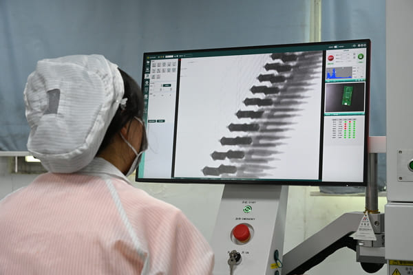
X-ray inspection is used for BGA and QFN packages with hidden connections. If a correctable defect is found, the affected board is reworked and inspected again before moving forward.
When required, programmable devices receive customer-provided firmware. Functional testing checks whether the PCBA performs as intended under agreed test conditions.
The test may confirm power behavior, input and output signals, communication functions, or other product-specific operations. The board then receives a final quality and quantity review before ESD-safe packaging and shipment.
When required, programmable devices receive the approved customer firmware, and boards undergo electrical or functional testing against agreed criteria. Final checks confirm workmanship, identification, quantity, and required records. Accepted assemblies are packed with ESD protection, cushioning, and moisture protection where specified.
Packaged assemblies are checked against the order for product identification, quantity, shipping labels, and delivery details. Required inspection or test documentation accompanies the shipment. The boards are then dispatched using the agreed shipping method, with tracking information provided when available.
Different PCB designs require different component mounting and soldering methods. PCBgogo supports multiple PCB assembly technologies, allowing the PCB manufacturing process to be selected according to component type, board construction, mechanical requirements, and order quantity. Below are some of the PCB assembly technologies supported by PCBgogo. For additional options, including advanced and high-precision assembly solutions, please contact us.
SMT assembly places electronic components directly onto pads on the PCB surface. It is well suited to compact products, high-density layouts, and designs that use miniature components. PCBgogo supports automated SMT assembly for both prototype and production orders.
Through-hole assembly is used for components whose leads pass through drilled holes in the PCB. It is commonly selected for connectors, transformers, large capacitors, switches, and components that require stronger mechanical attachment.
Depending on the board design and production requirements, PCBgogo can complete through-hole soldering through wave soldering or manual soldering. Manual processing is also useful for low-volume projects and components that require special handling.
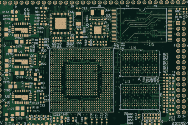
BGA, Micro-BGA, and QFN packages support high-density designs, but their hidden solder joints cannot be fully examined through visual inspection. PCBgogo provides assembly for these packages, along with X-ray inspection to verify solder joint quality.
PCBgogo also provides cable and wire harness assembly for projects that require connections between the PCBA and other parts of the finished product. Available options include custom cables, wiring harnesses, power leads, and cable assemblies for different electronic applications.
Cable specifications such as wire gauge, connector type, pinout, cable length, labeling, and electrical test requirements should be clearly defined in the production documents.
PCBgogo - Reliable, High-Quality PCB Manufacturing
Save time and money with an all-in-one solution for PCB fabrication, assembly, and parts. Reduce vendor coordination, avoid split shipments, and get consistent, reliable quality.
Get Free Quote >
Choosing the right PCB assembly partner involves more than comparing price and lead time. Technical capability, quality control, and reliable project support all affect the final result. PCBgogo provides flexible PCB assembly solutions for projects ranging from early prototypes to volume production. Here is what makes PCBgogo a reliable choice:
Wide range of PCB materials and board types: Assembly is available for FR-4, metal-core, rigid, flexible, and rigid-flex PCBs, supporting projects with different electrical, mechanical, and thermal requirements.
Advanced assembly technologies: PCBgogo supports SMT, through-hole, and mixed assembly, as well as BGA, Micro-BGA, QFN, and other fine-pitch packages.
Multiple quality inspections: Visual inspection, AOI, and X-ray inspection are used to identify component placement and soldering defects. IC programming and functional testing are also available according to project requirements.
From prototypes to volume production: Customers can use the same supplier for initial prototypes, design revisions, small-batch validation, and larger production orders.
Flexible component sourcing: PCBgogo can source all components, work with customer-supplied parts, or combine both options to suit the project.
Fast production and global delivery: Expedited assembly is available for eligible projects, with international shipping options for customers worldwide.
Whether you are building an initial prototype or preparing for volume production, PCBgogo can provide PCB manufacturing and assembly support tailored to your project. Upload your Gerber files and BOM today to receive a PCB assembly quote and start your project with PCBgogo.
The essential files are Gerber data, a complete BOM, pick-and-place or centroid data, and an assembly drawing. Schematics, firmware, test instructions, and special packaging requirements should also be supplied when relevant.
SMT components are mounted on surface pads and normally soldered by reflow. Through-hole component leads pass through drilled holes and are soldered manually or by wave soldering. A board can use either method or combine both.
Yes. PCBgogo lists BGA, Micro-BGA, and QFN among its supported packages. Because their solder joints are hidden beneath the components, X-ray inspection is used to evaluate placement and joint quality.
Functional testing is recommended when the behavior of the finished board must be verified, but its scope depends on the project. Customers should provide the test method, expected results, firmware, and any required fixtures or reference samples.
Lead time depends on board complexity, component availability, order quantity, inspection requirements, and testing. PCBgogo offers expedited assembly for eligible projects, but the schedule is confirmed after the production files and material status have been reviewed.
Submit consistent production files, use exact manufacturer part numbers in the BOM, mark component polarity clearly, identify acceptable substitutes, and provide testing requirements during the quotation stage. Early clarification prevents purchasing and production from being interrupted later.

 日本語
日本語
 한국어
한국어

