


Waiting weeks for a circuit board can slow down testing, delay a product demonstration, and push back a launch date. A quick-turn PCB service gives engineers a faster way to turn a digital design into a physical board.
Fast production still requires a manufacturable design, complete files, available materials, and an efficient engineering review.
This guide explains how quick turn PCB manufacturing works, what affects the schedule, and how to get your boards faster without taking unnecessary quality risks.
A quick turn PCB is a custom printed circuit board produced on an expedited manufacturing schedule. A straightforward prototype may be fabricated in as little as 24 to 48 hours. More complex boards can take several business days or longer.
The actual turnaround depends on the layer count, material, board dimensions, copper weight, via technology, surface finish, quantity, and testing requirements.
It is also important to distinguish between fabrication time and delivery time. A quoted 24-hour turnaround usually refers to manufacturing the bare board. It may not include engineering review, PCB assembly, weekends, shipping, or customs clearance.
Always confirm what the quoted turnaround includes before placing an order.
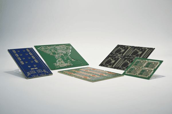
Quick turn manufacturing is commonly used during prototyping, design validation, pre-production, and urgent low-volume builds.
Faster design validation. A physical PCB lets engineers test electrical performance, thermal behavior, mechanical fit, and component placement. A shorter cycle makes the next design revision possible sooner.
Lower development risk. A small prototype batch can reveal problems before the company commits to volume production. Correcting five prototypes costs far less than reworking thousands of finished units.
Shorter time to market. Fast PCB prototyping gives hardware teams more testing time before customer demonstrations, certification appointments, or planned product launches.
Support for bridge production. A small quick turn order can supply beta units, replacements, or early customer shipments while full production is being prepared.
There is no universal lead time for every PCB design. A simple 2-layer rigid board uses fewer manufacturing steps than a multilayer HDI or rigid-flex PCB. Typical planning ranges include:
Simple 1- or 2-layer rigid boards: Eligible prototype designs may be fabricated within 24 to 48 hours.
Standard multilayer boards: These usually require several business days because the factory must process, align, laminate, drill, plate, and inspect multiple layers.
Flex and rigid-flex boards: These often have longer lead times because they require specialized materials and additional handling.
Assembled circuit boards: The schedule includes bare-board fabrication, component sourcing, assembly, inspection, and any requested testing.
These ranges are only planning estimates. The schedule shown for the exact design and selected options should be treated as the confirmed production time.
You should also ask when the manufacturing clock starts. Some suppliers begin counting after payment. Others begin only after the files pass engineering review and all technical questions have been resolved.
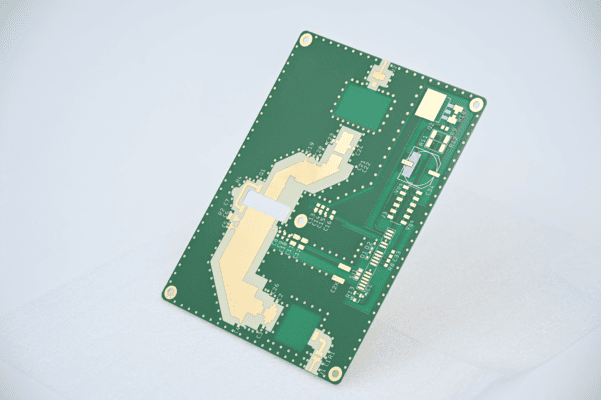
Understanding the main schedule drivers can help you avoid preventable delays.
Each additional layer increases the number of imaging, alignment, lamination, drilling, and inspection steps. A standard 4-layer stackup is usually easier to schedule than a custom 10-layer construction.
HDI boards may need multiple lamination cycles for blind, buried, or stacked microvias. A standard manufacturer-supported stackup is usually faster.
Standard FR-4 is widely available and often provides the shortest lead time. High-frequency laminates, high-temperature materials, metal-core substrates, and unusual dielectric thicknesses may need special sourcing.
Do not approve a material substitute without engineering review, especially for RF, thermal, or high-voltage designs.
Fine traces, narrow spacing, small holes, blind vias, buried vias, and via-in-pad structures require more advanced production processes. They may also require extra inspection.
Use advanced features only when needed. A standard through-hole via is usually faster and less expensive to produce.
Heavy copper requires different etching and plating controls. This can extend the production schedule, especially on boards with fine features.
Common finishes are easier to schedule than mixed finishes. Base the selection on electrical, assembly, and connector requirements.
Electrical testing, controlled-impedance verification, X-ray inspection, microsection analysis, and detailed quality documents all require time.
Do not remove necessary checks to save time. Include them in the original quote so they can be scheduled correctly.
Missing or conflicting information is one of the most avoidable causes of delay. Production may stop if the Gerber files, order form, and fabrication drawing show different specifications.
Clear files speed up review and reduce the risk of incorrect manufacturing assumptions.
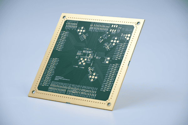
When deadlines are tight, getting reliable PCBs sooner helps you stay on schedule with testing and the next round of design revisions. PCBgogo offers 24-hour expedited production for eligible PCB orders, along with online production tracking to help you plan your next steps.
At PCBgogo, expedited orders follow the same strict quality standards. We never compromise on materials or skip essential manufacturing and inspection steps to meet a deadline. From base material selection and through-hole copper plating to automated optical inspection (AOI) and electrical testing, we carefully monitor every stage to ensure reliable quality for your quick-turn prototypes.
The table below outlines PCBgogo's quick-turn PCB production lead times:
| PCB Order Quantity (m2) | Original Lead Time (Days) | Current Lead Time (Hours) |
|---|---|---|
| 0- 50 pcs & < 1m2 | 2 - 3 Days | 24 Hours |
| 1m2 - 5m2 | 5 - 6 Days | 3 - 4 Days |
| 5m2 - 10m2 | 6 - 7 Days | 4 - 5 Days |
| More than 10m2 | 8 - 10 Days | 5 - 6 Days |
For advanced PCBs, a dependable turnaround starts with getting the manufacturing details right. PCBgogo supports HDI, multilayer, rigid-flex and high-frequency designs through our own production facilities, experienced engineering support and material options from suppliers such as Rogers, Shengyi and ITEQ. Before production, our engineers review the stack-up, via structures, impedance requirements and material availability to address potential manufacturing issues early. Careful process control, inspection and electrical testing support consistent quality as your project moves from prototype to production. The table below outlines our advanced PCB production lead times to help you plan testing and assembly, with the final schedule confirmed according to your design complexity, material requirements and order quantity.
| PCB Layers | PCB Order Quantity (m2) | Original Lead Time (Days) | Current Lead Time (Hours) |
|---|---|---|---|
| 2 Layers | <1 m2 | 5 Days | 48 Hours |
| 1-5 m2 | 7 Days | ||
| >5 m2 | 8 Days | ||
| 4 Layers | <1 m2 | 5 Days | 48 Hours |
| 1-5 m2 | 7 Days | ||
| >5 m2 | 12 Days | ||
| 6 Layers / 8 Layers | <1 m2 | 7 Days | 72 Hours |
| 1-5 m2 | 9 Days | ||
| >5 m2 | 12 Days | ||
| 10 Layers | <1 m2 | 10 Days | 96 Hours |
| 1-5 m2 | 10 Days | ||
| >5 m2 | 15 Days | ||
| 10 or more Layers | <1 m2 | 10 Days | 96 Hours |
| 1-5 m2 | 10 Days | ||
| >5 m2 | 15 Days |
PCBgogo - Reliable, High-Quality PCB Manufacturing
Save time and money with an all-in-one solution for PCB fabrication, assembly, and parts. Reduce vendor coordination, avoid split shipments, and get consistent, reliable quality.
Get Free Quote >
A well-prepared order can save more time than choosing the most expensive rush option.
Run a design rule check before export. Compare the critical dimensions and clearances with the manufacturer's capabilities.
Do not assume that the default rules in your PCB design software match the selected production process.
Include Gerber and NC drill files, a clear outline, layer information, fabrication notes, and all material and impedance requirements.
Remove obsolete files before creating the final ZIP folder. Extra design versions can create confusion during review.
The quote details must match the production files. Conflicting copper weights, thicknesses, or finishes will trigger an engineering question.
Review the complete package as if you were the engineer receiving it for the first time.
Assign someone to monitor the order portal and email after submission. A production slot may be available, but the manufacturer cannot proceed while waiting for approval.
For U.S. customers working across time zones, a delayed response can add a full business day.
PCBgogo has served global PCB customers since 2015. Its services include quick-turn prototypes, advanced boards, component sourcing, and turnkey assembly.
Eligible prototype designs may be available with production in as little as 24 hours. Because the actual lead time depends on the board specifications, customers should confirm the manufacturing option displayed for their exact order.
PCBgogo also reviews submitted orders through its engineering team before production. This review helps identify missing information or manufacturing concerns before the board reaches the factory floor.
Its online quote system shows pricing and available production options based on the specifications entered by the customer.
Check the design. Review the board against the appropriate manufacturing rules and export the final production files.
Request an online quote. Visit the PCBgogo online PCB quote page and enter specifications that match the design.
Select a production option. Choose an available quick-turn schedule and upload the fabrication or assembly package.
Confirm the complete schedule. Review the price, production time, shipping method, and estimated delivery date before payment.
A successful quick-turn PCB project begins with a manufacturable design and a complete set of files. Standard materials, proven stackups, available components, and fast communication can all shorten the schedule.
PCBgogo combines online quoting, engineering review, PCB fabrication, component sourcing, and assembly in one manufacturing workflow. Upload your design today to review the available turnaround options and move your next prototype from the screen to the test bench faster.

 日本語
日本語
 한국어
한국어

