
 日本語
日本語
 한국어
한국어

How to Design and Build a Custom Arduino Shield PCB?
If you have ever finished an Arduino prototype on a breadboard and then stared at the tangle of jumper wires wondering how to turn it into something robust, you are not alone. Breadboards are great for experimentation, but they introduce intermittent connections, signal noise, and size constraints that make any real project unreliable.
This guide walks through everything you need to know about designing and building a custom Arduino shield PCB, from pin mapping and schematic capture through layout, fabrication, and assembly.
What Is a Custom Arduino Shield PCB?
A custom Arduino shield PCB is a purpose-built expansion board designed with header connectors that precisely match the Arduino pin layout, allowing it to be mounted directly on top of an Arduino board. Unlike generic development boards, custom shields integrate application-specific circuits for functions such as motor control, wireless communication, sensor integration, GPS positioning, and relay control. Built on Arduino’s widely adopted open hardware ecosystem, shield PCBs provide engineers and makers with a flexible way to prototype and develop customized embedded solutions.
The key advantage of a custom shield over a generic prototyping board is that every component, trace, and connector is placed for a single purpose. The result is a smaller, more reliable, and more professional finished product than anything a breadboard or perfboard can achieve.
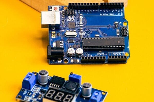
Applications of Arduino Shield PCBs
The specific application determines which components, layout constraints, and layer count make sense for your shield design:
IoT sensor hub: A shield that breaks out multiple I2C and SPI sensor ports with onboard voltage regulation, level shifting, and an SD card slot for offline data logging. A dedicated 3.3V LDO regulator powers low-voltage sensors without overloading the Arduino's onboard 3.3V pin, which is rated for only 50 mA.
Motor and actuator driver: A shield carrying an L298N or DRV8833 dual H-bridge IC with screw terminals for DC motors, flyback diodes for inductive kickback protection, and a dedicated high-current power input separate from the Arduino's barrel jack. PWM-capable pins (D3, D5, D6, D9, D10, D11 on the Uno) are routed with wider 20 mil or greater traces to handle motor current.
Relay control board: A shield with four or eight SPDT relays, optocoupler isolation between the relay coils and the Arduino GPIO pins, and flyback protection diodes. Without optocouplers, the inductive spike from a relay coil switching can reset or damage the Arduino's microcontroller.
Wireless communication shield: A shield integrating an nRF24L01, LoRa SX1278, or ESP8266 module with a dedicated 3.3V regulator capable of supplying the peak transmit current (typically 120 mA for an nRF24 at full power) and a u.FL connector for an external antenna.
Data acquisition and ADC shield: A shield featuring a high-resolution external ADC such as the ADS1115 (16-bit) with proper analog grounding and a guard ring layout. The Arduino's built-in 10-bit ADC is insufficient for applications like strain gauge reading or thermocouple measurement.
Each of these applications makes a different set of demands on the PCB design. A motor shield prioritizes high-current trace routing and thermal management, while an ADC shield prioritizes low-noise analog layout and ground plane integrity.
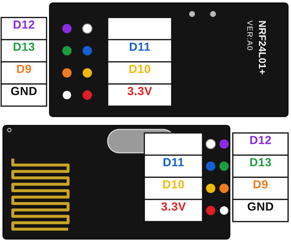
PCB Design and Pin Details
The pinout is the mechanical backbone of any shield: if header positions or pin assignments are wrong, the board will not fit or function. The table below summarizes the Uno R3 pin headers and their key design considerations:
| Header | Pins | Key Design Notes |
|---|---|---|
| Digital I/O (top, 8-pin) | D0–D7 | D0/D1 shared with UART; avoid as general I/O if using Serial |
| Digital I/O (top, offset) | D8–D13, GND, AREF | D13 drives onboard LED via buffer; verify drive strength for SPI SCK |
| Analog input (bottom, 6-pin) | A0–A5 (also D14–D19) | A4/A5 are I2C SDA/SCL with onboard 10k pull-ups to 5V |
| Power (bottom, 8-pin) | IOREF, RESET, 3.3V, 5V, GND×2, VIN | 3.3V limited to 50 mA; VIN carries barrel jack input (7–12V) |
| ICSP (end, 2×3 pin) | MISO, VCC, SCK, MOSI, RESET, GND | Direct SPI access; used for ISP programming or auxiliary MCUs |
Shield Mechanical Dimensions
The Arduino Uno R3 PCB measures 68.6 mm by 53.3 mm. A standard shield matches these dimensions, with M3 mounting holes at each corner positioned 2.7 mm inward from the edges. The four header strips must align to a spacing of 40.6 mm center-to-center between the top digital row and the bottom power row, with the analog row spaced 12.7 mm inward from the power row. Account for vertical clearance above the USB connector (10.5 mm) and barrel jack (11.5 mm). For underside components, maintain at least 8 mm clearance above the ATmega328P DIP socket.
How to Design a Custom Arduino Shield PCB
The design workflow moves from concept to manufacturing files in six stages:
Step 1: Define requirements and select components. List every function the shield must perform, then translate each into specific part numbers. Check availability and lead times before opening the PCB editor; a component on 12-week backorder delays the entire project.
Step 2: Capture the schematic. Place Arduino header symbols as connectors, then add each functional block one at a time. Use net labels for power rails rather than drawing long wires across the sheet. Add a 100 nF decoupling capacitor near each IC power pin, and buffer any pin carrying more than 40 mA (the ATmega328P per-pin maximum) with a transistor or MOSFET. KiCad (free, open source, with an Arduino shield template library) is a widely used EDA tool for shield design, handling schematic capture and PCB layout in one application.
Step 3: Define the board outline and place headers. Set dimensions to 68.6 mm × 53.3 mm for a full-size shield, or customize for your enclosure. Place the four Arduino header footprints at their exact mechanical positions first; they are the fixed reference points of the design.
Step 4: Place components and route traces. Group components by function: keep analog front-ends away from digital switching sections. Route high-current traces at 0.5 mm (20 mil) width per ampere for 1 oz copper; signal traces at 0.25 mm (10 mil). Use a solid bottom-layer ground plane and avoid 90-degree trace bends in favor of 45-degree corners.
Step 5: Run Design Rule Check (DRC). Configure constraints from your fabricator: typically 6 mil minimum trace width and clearance, 0.3 mm minimum drill, 4 mil minimum annular ring. Resolve every DRC error before exporting; unresolved clearance violations cause shorts, and drill violations cause file rejection.
Step 6: Generate Gerber files and BOM. Export RS-274X Gerber files for each copper layer, solder mask, silkscreen, and board outline, plus an NC drill file. Generate a BOM listing every component by reference designator, manufacturer part number, and footprint. Verify the board outline matches intended dimensions before uploading; a tool like PCBgogo's online Gerber viewer lets you preview every layer visually before committing to production, catching outline or drill mismatches before they become a manufacturing delay.
PCB Assembly Methods
Once fabricated PCBs arrive, you have three assembly options. The table below compares them across key practical factors:
| Method | Best For | Component Types | Skill Level | Relative Cost |
|---|---|---|---|---|
| Hand soldering | Prototypes, low volume (1–5 pcs) | Through-hole, SOIC, 0805, 0603 | Beginner–Intermediate | Lowest |
| Hot plate/reflow oven | SMD-dominant boards, medium volume | QFP, QFN, 0402, SOT-23 | Intermediate | Low (equipment cost) |
| Professional SMT (PCBA) | Production runs, fine-pitch/BGA | All packages including BGA, 0201 | None (outsourced) | Moderate–High |
Hand soldering: Use a temperature-controlled iron at 320–350°C with a 0.5 mm tip. Solder from shortest components upward, finishing with tall connectors. Lead-free solder requires higher temperatures (360–380°C) and flows less readily than leaded solder.
Reflow soldering: Apply solder paste via stencil, place components, then follow the paste manufacturer's temperature profile (ramp to 150°C, soak at 150–180°C for 60–120s, peak at 210–230°C for 30–60s). Produces consistent joints for packages difficult to hand-solder.
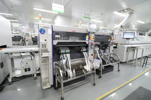
Professional SMT assembly: A PCBA service handles stencil printing, automated pick-and-place, reflow, and AOI inspection. Turnkey services also procure components, eliminating separate distributor orders and reducing counterfeit-part risk. This is the only practical option for BGA packages, which require X-ray inspection.
Regardless of method, clean the finished board with 99% isopropyl alcohol to remove flux residue that can absorb moisture and create leakage paths between pins.
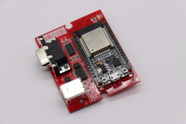
Arduino Shield PCB and PCBA Manufacturer: How PCBgogo Supports Custom Shield Projects
Once your design is validated, the fabrication partner you choose determines whether Gerber files become reliable boards on schedule or a source of delays. For custom Arduino shield projects spanning simple two-layer through-hole boards to dense multi-layer SMD assemblies, PCBgogo offers services that align directly with these needs:
Rapid prototyping with low minimums: Standard PCB orders start from 1 piece, and PCBA orders from just 1 piece, with 24-hour quick-turn available for FR-4 prototype boards. This allows multiple design iterations within a single week.
Multi-layer fabrication up to 14 layers: Covers the two-to-four-layer range most shield projects use, with headroom for complex mixed-signal or impedance-controlled designs.
DFM review before production: PCBgogo's engineers check for insufficient annular rings, trace width issues, and copper-to-edge clearance violations. For shields, common flags include pad size problems on header pins that carry mechanical insertion stress.
Turnkey PCBA with SMT lines: Component procurement, stencil fabrication, automated placement, reflow soldering, and AOI inspection are all handled in-house. Standard packages (SOIC, QFP, 0603, 0805) are routed through daily production without setup fees.
Free stencils with assembly orders: Laser-cut stainless steel stencils available in frameless, framed, or electroformed options for designers who prefer in-house assembly.
Common Design Pitfalls and How to Avoid Them
Reversed header orientation: The single most common mistake. The digital pins should face the USB connector edge. Print a 1:1 paper template and test-fit on a real Arduino before ordering.
Missing IOREF connection: Shields designed for both 3.3V and 5V Arduino variants must reference IOREF rather than hardwiring to 5V; otherwise, stacking on a 3.3V board like the Due will damage components.
Insufficient underside clearance: Components under the shield must clear the USB connector (10.5 mm) and the ATmega328P DIP package. Keep underside SMD parts under 2 mm height and away from the connector zone.
5V regulator overload: The Arduino's onboard NCP1117 regulator supplies approximately 400–500 mA after its own consumption. If shield peripherals draw more, add a dedicated regulator powered from VIN.
Floating reset pin: If unused, tie the RESET pin to 5V with a 10k pull-up resistor to prevent noise-induced resets.
Frequently Asked Questions
What is the difference between an Arduino shield and a breakout board?
A shield stacks directly onto Arduino pin headers and matches its mechanical form factor. A breakout board connects via jumper wires without conforming to the Arduino's footprint, offering more placement flexibility but adding wiring complexity.
Can I design an Arduino shield that works with both the Uno and the Mega?
Yes. The Mega uses the same outer header spacing as the Uno. If your shield fits within the Uno's 68.6 mm × 53.3 mm outline, it clears the Mega's extended PCB without interfering with its additional headers.
Do I need a ground plane on my Arduino shield PCB?
A continuous ground plane on at least one layer is strongly recommended. It provides a low-impedance return path for signals, reduces EMI, and improves decoupling capacitor performance by lowering inductance to the IC ground pin.
How much does it cost to fabricate a custom Arduino shield PCB?
Prototype quantities (1–10 pieces) of a two-layer shield typically range from $2 to $15 total including shipping, depending on turnaround time and surface finish. Assembly adds cost based on component count, package types, and sourcing method.
Can I use surface-mount components if I am hand soldering?
Yes, with hand-solderable packages: SOIC, 0805, 0603, and SOT-23 are manageable with a fine-tip iron. Avoid QFN, BGA, and 0402 or smaller passives for hand soldering; these require reflow equipment.
Conclusion
A custom Arduino shield PCB turns a fragile breadboard prototype into a compact, reliable, and repeatable device. The design process (schematic capture, pin mapping, component placement, routing, DRC, and Gerber export) follows a logical progression where each stage validates the previous one. Choosing a fabrication partner like PCBgogo that offers rapid prototyping, DFM review, and turnkey assembly keeps the transition from design files to working boards fast and low-risk.
Upload your Gerber files and BOM now for a quote, and get your shield PCB project started with PCBgogo.





