日本語
日本語
 한국어
한국어
Why Choose PCBgogo?


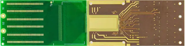
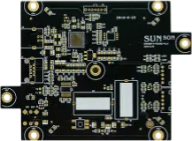
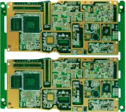
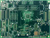
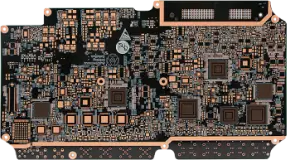
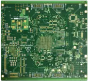
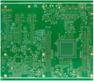
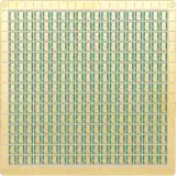
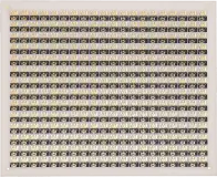
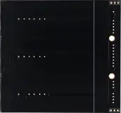
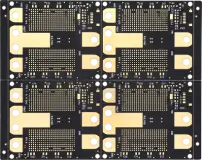
Advanced PCB Showcase
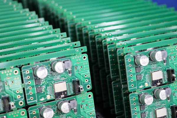
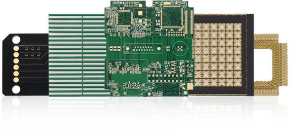
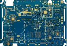
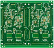
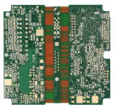
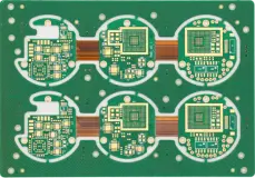
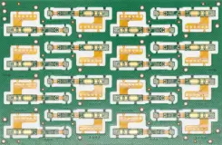
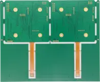
PCBgogo delivers advanced PCB manufacturing for designs that demand greater precision, tighter tolerances, and dependable electrical performance. Our capabilities support complex technologies such as multi-stage HDI, blind and buried vias, fine-line routing, controlled impedance, high-frequency materials, heavy copper construction, and rigid-flex structures. From compact consumer devices to industrial control, 5G communications, medical equipment, and automotive electronics, we manufacture complex PCBs built for high-density, high-speed, and reliable performance. Whether your project requires compact layouts, stable high-frequency signals, improved thermal performance, or high-current capability, PCBgogo helps turn challenging PCB designs into production-ready boards.
resistor-circuit-board
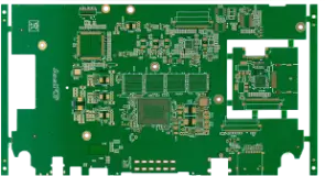
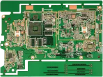
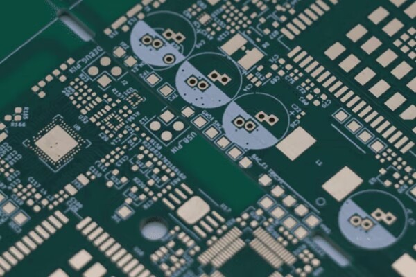
immersion-gold
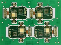
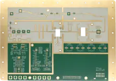
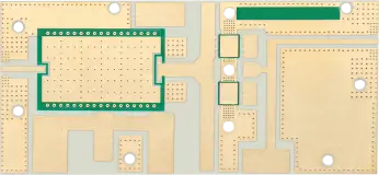
| Item | Standard PCB | Advanced PCB |
|---|---|---|
| Material | Standard FR-4 | High-Tg, low-loss, RF, thermally enhanced materials |
| Typical Applications | Consumer electronics, Household devices, Basic control boards, General-purpose electronics | 5G communications, RF & microwave, Medical equipment, Automotive electronics, Industrial control, Aerospace, High-performance computing, Compact smart devices |
| Typical Board Structures | Single-sided, Double-sided | HDI, Multilayer, Rigid-flex, RF, High-speed, Heavy-copper, IC substrates |
| Drilling | Mechanical holes: ≥0.20 mm | Mechanical holes: ≥0.15 mm, Laser vias: ≥0.10 mm |
| PTH Copper | ≥20μm | ≥18μm |
| Power and Thermal Management | General thermal requirements | Heavy copper structures, High-current designs, Improved heat dissipation, Thermal management |
| Manufacturing Complexity | Conventional stackups, standard PCB fabrication | Complex stackups, Lamination, Impedance control, Customer-specific requirements |
| Test method | AOI, electrical testing | AOI, Electrical, Flying-probe/fixture, Impedance, Microsection, Custom testing |
| Glass transition ℃ | >130℃ | >140℃ |
| Routing and Interconnect Density | Conventional trace widths/spacing, Through-hole interconnects | Fine-line routing, Fine-pitch, Microvias, Blind/buried vias, Multi-stage HDI |
| Signal Performance | General electronic signals, Standard circuit requirements | Controlled impedance, High-speed signal integrity, Low-loss transmission, Stable RF performance |
| Standard | IPC requirements, customer specifications | IPC Class 2/3 reliability, Specific reliability requirements |
| Documentation and Packaging | Standard documentation, Standard packaging | Inspection/test reports, CoC, MSL packaging, Custom packaging |
| Cleanliness | Meet IPC standards | Beyond IPC requirement |
| Certification | UL, ISO9001:2015, RoHS etc. | UL, ISO9001:2008, ISO14001:2004, ISO/TS16949:2009, RoHS etc. |
Material & Processing Options
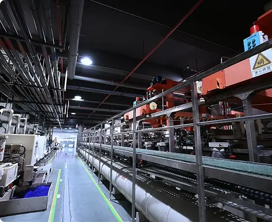
As printed circuit board technology evolves and electronics keep shrinking, it is vital to select matching base materials, surface finishes and extra fabrication options. Our facility owns professional equipment to implement all specialty processes for advanced HDI circuit board designs.
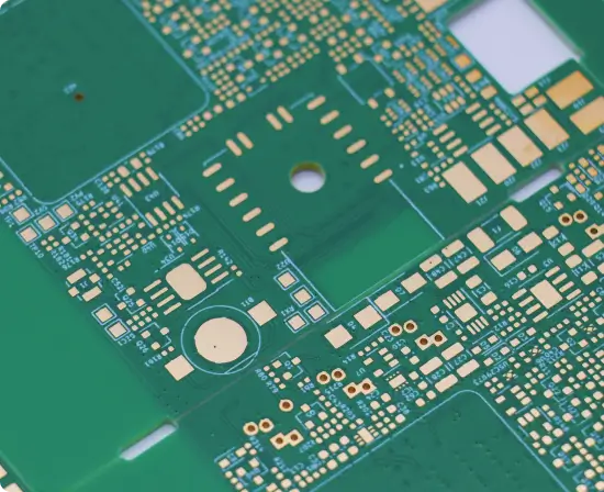
- Layer Count: 1-40 layers.
- Finished Copper Thickness: 0.5–6 oz.
- Materials: Isola 370HR, ITEQ IT180A, Shengyi S1000-2M and S1170G, etc.
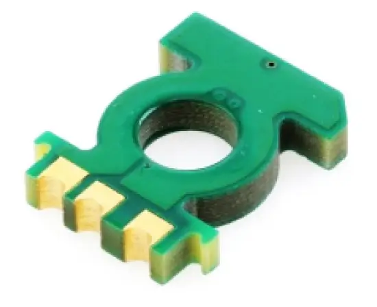
- Surface Finishes: ENIG, HASL, lead-free HASL, OSP, immersion tin, immersion silver, hard gold, and gold fingers.
- Maximum PCB Size: Single-sided and double-sided PCBs: 600 × 1200 mm, Multilayer PCBs: 560 × 1150 mm.
Capabilities of PCBgogo
PCBgogo provides flexible manufacturing solutions for advanced PCB designs, from material selection and surface finishes to specialized fabrication processes. Our capabilities support HDI, Rogers and RF PCBs, rigid-flex boards, heavy copper PCBs, and other complex multilayer designs that require high density, controlled impedance, reliable thermal performance, and consistent quality.
| Category | Item | Capability |
|---|---|---|
| PCB Types & Layers | Rigid PCB | 1-40 layers |
| Metal-Core PCB | 1-2 layers | |
| HDI PCB | 4-14 layers | |
| Rogers PCB | 1-14 layers | |
| Materials | FR-4 | Yes |
| High TG | Up to Tg 170 | |
| Halogen Free | Yes | |
| High Frequency | Yes | |
| Max PCB size | Single-layer and double-layer: 600*1200mm Multi-layers: 560*1150mm | |
| PCB thickness |
1 Layer/2 Layers: 0.2~2.4mm
4 Layers: 0.4~2.4mm 6 Layers: 0.8~2.4mm 8 Layers: 1.0~2.4mm 10 Layers: 1.2~2.4mm Note: Customized PCB thickness and Layer stack up are acceptable. |
|
| Min width | 3mils | |
| Min space | 3mils | |
| Outer Layer Copper Thickness |
1oz/2oz/3oz (35μm/70μm/105μm)
Note: 2oz PCB thickness≥1.2mm, Via size≥0.25mm, Min Track/Spacing≥0.15mm 3oz PCB thickness≥2.0mm, Via size≥0.3mm, Min Track/Spacing≥0.2mm |
|
| Inner Layer Copper Thickness | 1oz/1.5oz (35μm/50μm) | |
| Min CNC finished aperture | 0.15mm | |
| Min Laser finished aperture | 0.1mm | |
| Max aspect ratio | 12 : 1 | |
| Solder mask color | Green/Red/Yellow/Blue/White/Purple/Black/Matte black/Matte green/None | |
| Impedance control tolerance | Yes | |
| Min annular ring | 3mil | |
| Panelization | V-scoring, Tab-routing, Tab-routing with Perforation (Stamp Holes) |
Explore detailed PCB manufacturing capabilities, including layer count, material options, copper thickness, drilling, tolerances, surface finishes, and advanced fabrication processes. For complex or custom PCB requirements, contact via service@pcbgogo.com for tailored manufacturing support.
Application Solutions
Specialized in high-precision circuit board technology, we provide full-process, one-stop services to meet strict industrial manufacturing standards.

Consumer Electronics
HDI, flexible PCBs (FPCs), and rigid-flex PCBs are widely applied in smartphones, tablets, wearable devices, AR/VR products, and laptops for compact, integrated consumer devices.
Read More >
Medical Devices
Stable, low-noise, and highly reliable PCBs are used in CT and MRI systems, ultrasound equipment, patient monitors, surgical robots, and in-vitro diagnostic devices.
Read More >
Automotive Electronics
High-reliability PCBs are essential for smart cockpits, autonomous-driving domain controllers, electric-drive systems, battery management systems, and in-vehicle radar.
Read More >
Industrial Control
Advanced PCBs are used in PLCs, industrial robots, machine-vision systems, frequency converters, CNC equipment, and smart-grid systems.
Read More >
Servers & Data Centers
High-speed, high-power, and thermally efficient PCBs support AI servers, GPUs, accelerator cards, storage systems, and networking equipment with reliable processing and cooling.
Read More >
Aerospace & Defense
High-reliability, multilayer, high-frequency PCBs are applied in avionics, satellite systems, airborne radar, guidance systems, unmanned aerial vehicles, and naval electronics.
Read More >
New energy systems
Thick-copper and high-power PCBs are commonly used in photovoltaic inverters, energy-storage systems, EV charging stations, wind-power controllers, and BMS solutions.
Read More >
Security & Surveillance
Multi-layer & fine-line PCBs for IP cameras, video servers, access control systems and intelligent surveillance equipment with stable signal transmission.
Read More >Resource Hub


What is an advanced PCB?
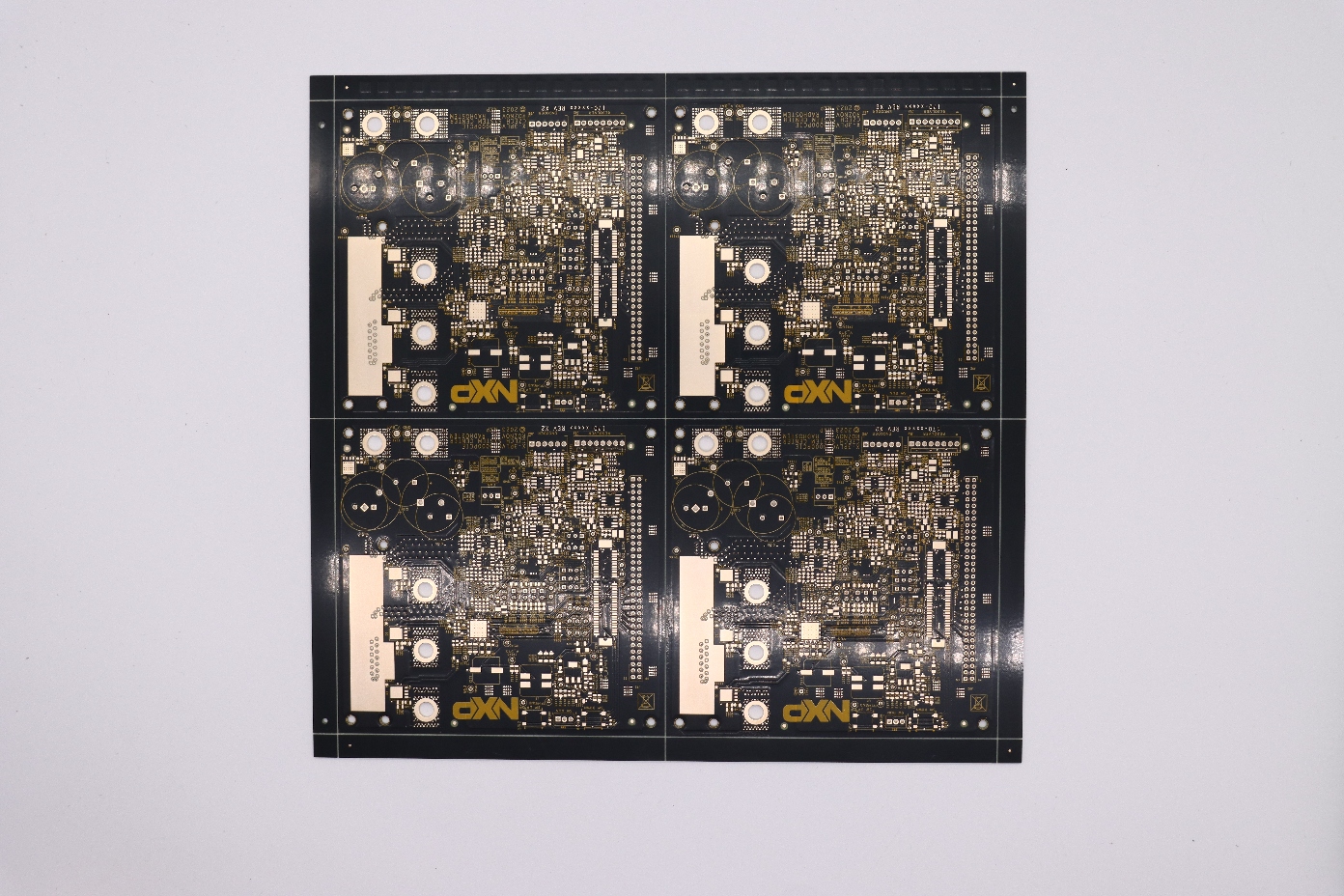
Advanced PCBs refer to high‑performance circuit boards including HDI, rigid‑flex, multilayer, fine‑line and high‑frequency boards, designed for miniaturization, high‑speed signal and high‑reliability application scenarios.
What files are needed for an advanced PCB quote?
Provide Gerber or ODB++ files, drill files, a board outline, stackup details, and impedance requirements when applicable.
Can PCBgogo provide PCB assembly for advanced PCB projects?
Yes. PCBgogo provides one-stop PCBA services that combine PCB fabrication, component sourcing, and assembly in one coordinated workflow. Our experienced team supports advanced PCB projects from prototype validation through production, helping reduce handoffs, improve quality control, and speed up delivery.
Can PCBgogo manufacture PCBs with blind, buried, and microvias?
Yes. We support advanced via structures for HDI and high-density PCB designs, with the final process confirmed through a manufacturability review.
What is the typical lead‑time for advanced PCB prototypes and mass production?
Prototype lead‑time for advanced PCBs ranges from 3-5 days depending on design complexity and material availability. For urgent projects, we also provide 24-hour expedited service. Mass‑production lead‑time will be confirmed in formal quotation.
Do you offer stack‑up design suggestion for high‑speed advanced PCBs?
Of course. Before production, PCBgogo’s experts review your order for manufacturability and provide practical recommendations and optimization solutions to support reliable production and strong product performance.
What materials can be used for advanced PCB manufacturing?
Common options include Shengyi S1141 and S1000-2M, Kingboard KB6160A and KB6160C, ITEQ IT180A, and Rogers. We also support PI and PET for flexible PCBs, polyimide with FR-4 for rigid-flex PCBs, and many more material options, contact us via service@pcbgogo.com to select the best fit for your design.
What factors will affect advanced PCB final cost?
Layer count, minimum trace & space, board thickness, material type, surface finish, panel size, testing and order quantity are the main factors.