



 日本語
日本語
 한국어
한국어

What Is PCB Assembly? Process, Methods & Services
PCB assembly (PCBA) is the process of mounting and soldering electronic components onto a bare printed circuit board to turn it into a functional electronic product. A bare PCB is just copper traces on laminate. It does nothing until resistors, capacitors, ICs, and connectors are attached through solder paste printing, component placement, reflow or wave soldering, inspection, and electrical testing.
I have worked with PCB assembly projects for years, helping engineers and businesses understand the process, choose the right assembly methods, and avoid common manufacturing issues. This guide walks through everything that happens between uploading your design files and receiving a tested, working board: the assembly methods, the step-by-step production flow, the files you need to prepare, service models, cost drivers, and what actually separates a reliable PCB assembly manufacturer from a risky one.
What Is PCB Assembly? PCBA vs. Bare PCB Fabrication
PCB assembly and PCB fabrication are two different manufacturing stages, and mixing them up is one of the most common sources of confusion when engineers request quotes.
PCB fabrication builds the bare board. Copper is etched into traces, layers are laminated, holes are drilled and plated, solder mask and silkscreen are applied, and a surface finish such as HASL or ENIG protects the exposed pads. The output is an unpopulated board with no components on it.
PCB assembly populates that bare board. Components are soldered onto the pads and through-holes, then the board is inspected and electrically tested. The output is a PCBA, a printed circuit board assembly that can actually power on and perform its designed function.
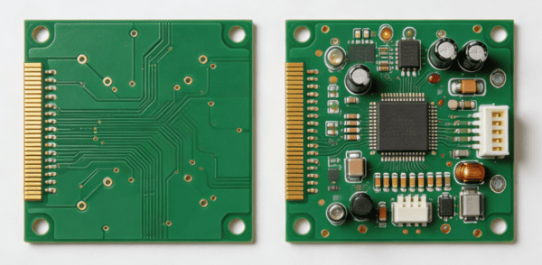
A simple way to remember the difference: fabrication makes the board, assembly makes the product. When you order a “PCBA” or a “PCB assembly service,” you are ordering both stages plus component sourcing, either from one vendor or from separate suppliers.
Why does this distinction matter in practice? Because responsibility for defects depends on it. A short circuit caused by a copper sliver is a fabrication defect. A tombstoned resistor is an assembly defect. When fabrication and assembly happen at different companies, diagnosing a failed board can turn into weeks of finger-pointing. This is the main reason many engineering teams now prefer one-stop suppliers that handle fabrication, component sourcing, and assembly under a single quality system.
PCB Assembly Methods: SMT, THT, and Mixed Assembly
Every assembly job uses one of three approaches, and the choice is dictated by the components in your bill of materials, not by preference.
Surface Mount Technology (SMT)
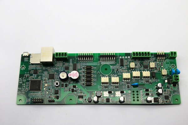
SMT places components directly onto pads on the board surface. It is the dominant method in modern electronics because it supports tiny packages (down to 01005 passives), enables placement on both sides of the board, and runs on fully automated high-speed lines. Fine-pitch ICs, BGAs, QFNs, and nearly all modern semiconductors are surface mount parts.
Through-Hole Technology (THT)
THT components have leads that pass through drilled holes and are soldered on the opposite side. The plated barrel grips the lead mechanically, which makes through-hole joints far stronger under physical stress. Connectors, transformers, large electrolytic capacitors, and parts that get plugged, pulled, or vibrated are still routinely through-hole for exactly this reason.
Mixed Assembly
Most real-world boards combine both: SMT for the dense circuitry, THT for connectors and power components. The standard sequence is SMT first (reflow soldering), then THT (wave, selective, or hand soldering), because a board that has already been through reflow can still accept through-hole parts, but not the other way around.
| Aspect | SMT | THT | Mixed |
|---|---|---|---|
| Component mounting | Components mounted directly on surface pads | Components inserted through drilled holes with leads | Combines surface-mount and through-hole components |
| Soldering method | Reflow soldering using solder paste and controlled heating | Wave soldering, selective soldering, or manual soldering | Reflow soldering first, followed by wave or selective soldering |
| Mechanical strength | Moderate mechanical strength | High mechanical strength due to through-hole connections | High strength where reinforced components are required |
| Miniaturization | Excellent support for compact packages such as 01005, BGA, and QFN | Limited due to larger component sizes and drilled holes | Depends on the overall PCB design and component mix |
| Automation level | Highly automated with pick-and-place machines | Partially automated or may require manual assembly | Uses combined automated SMT and THT production lines |
| Typical use | Consumer electronics, IoT devices, and computing products | Connectors, power electronics, and high-vibration applications | Most commercial and industrial electronic products |
If you are designing a new board, favor SMT parts wherever function allows. They reduce parasitic inductance, shrink the board, and cut assembly cost because automated placement is far cheaper per joint than hand or selective soldering.
The PCB Assembly Process Step by Step
Below is the production flow used by professional assembly houses. Understanding each stage helps you write better assembly notes and interpret quality reports when something goes wrong.
The steps that follow cover everything from a bare, fabricated board to a tested PCBA. They assume the bare PCB has already been manufactured. If you want to understand how the board itself is made, from copper etching and lamination through drilling and surface finishing, see our detailed guide to the PCB manufacturing process.
Step 1: DFM/DFA Review and File Verification
Before any solder paste touches a board, engineers verify the Gerber files, BOM, and pick-and-place data against each other. A design for assembly (DFA) check looks for problems like insufficient pad-to-pad clearance, wrong footprints, missing polarity marks, and parts placed too close to the board edge. Catching a footprint mismatch here costs an email. Catching it after reflow costs a production run.
Step 2: Solder Paste Printing
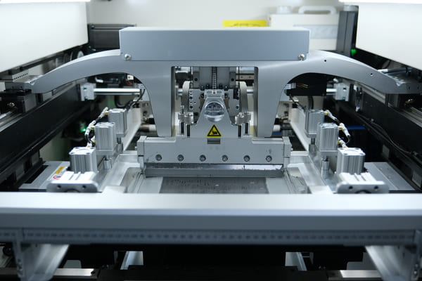
A laser-cut stainless steel stencil is aligned over the bare board, and solder paste (powdered solder alloy suspended in flux) is squeegeed across it, depositing a controlled volume of paste on every SMT pad. Stencil aperture design and paste volume control at this stage determine a large share of final solder joint quality. Industry experience consistently attributes the majority of SMT defects to problems that originate in paste printing.
Step 3: Solder Paste Inspection (SPI)
3D SPI machines measure the height, area, and volume of every paste deposit and compare it against the design. Boards with insufficient paste, bridging, or offset deposits are pulled and reprinted before components go on. Skipping SPI to save time is a false economy; defects caught here cost almost nothing to fix.
Step 4: Pick and Place
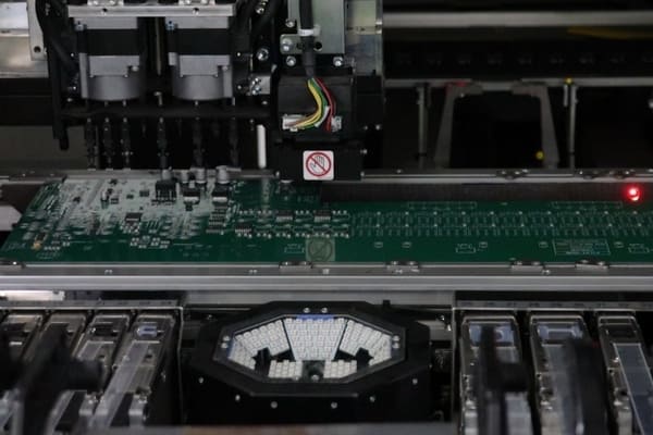
Automated pick-and-place machines pull components from reels, tubes, and trays, verify them by vision system, orient them, and set them onto the wet solder paste at rates of tens of thousands of components per hour. Placement accuracy for fine-pitch BGAs and 0201/01005 passives depends on both machine capability and the quality of your centroid (CPL) file.
Step 5: Reflow Soldering
The populated board travels through a multi-zone reflow oven following a controlled thermal profile: preheat, soak, reflow peak, and cooling. The paste melts, wets the pads and component terminations, and solidifies into permanent solder joints. Lead-free profiles typically peak around 235 to 250°C. A poorly tuned profile causes tombstoning, cold joints, and voiding, which is why serious assemblers profile each new board design rather than reusing a generic recipe.
Step 6: Automated Optical Inspection (AOI) and X-Ray
AOI cameras scan every board against a golden reference image, flagging missing parts, misalignment, wrong polarity, solder bridges, and insufficient solder. For packages with hidden joints, such as BGAs and QFNs, X-ray inspection reveals voids, bridging, and head-in-pillow defects that no optical system can see.
Step 7: Through-Hole Assembly
THT components are inserted manually or by machine, then soldered by wave soldering (high volume), selective soldering (targeted joints on mixed boards), or hand soldering (prototypes and delicate parts). Sensitive through-hole parts that cannot survive a solder wave should be flagged in your assembly notes so the assembler hand-solders them.
Step 8: Cleaning
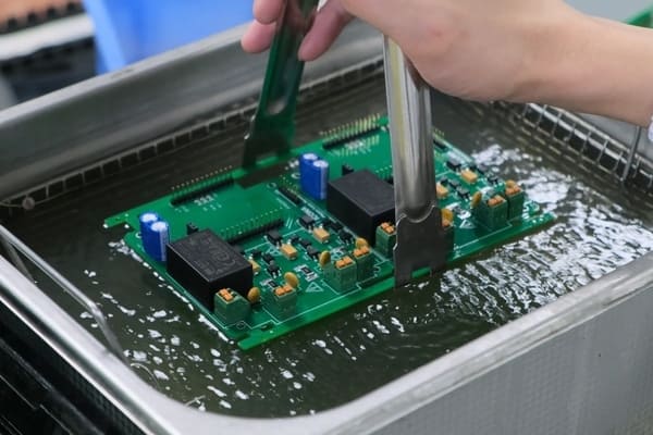
Flux residues are removed with deionized water washing or solvent cleaning where required. No-clean flux processes skip this step, but boards destined for conformal coating or high-impedance analog circuits usually need a genuine wash.
Step 9: Electrical Testing
Depending on volume and requirements, boards go through flying probe testing (flexible, no fixture cost, ideal for prototypes and small batches), in-circuit testing (ICT, fast per-board testing for volume production, requires a bed-of-nails fixture), and functional testing (FCT) that powers the board and exercises it the way the end product will.
Step 10: Final Inspection, Coating, and Packaging
A final quality inspection against IPC-A-610 acceptance criteria checks workmanship. Optional conformal coating protects boards used in humid, dusty, or corrosive environments. Finished assemblies are then vacuum-packed with desiccant and ESD protection for shipment.
Files You Need Before PCB Assembly Starts
Incomplete or contradictory files are the number one cause of assembly delays, ahead of component shortages. Three files are mandatory:
Gerber files (or ODB++). These define every fabrication layer: copper, solder mask, silkscreen, paste, and drill data. They drive both board fabrication and stencil cutting.
Bill of Materials (BOM). A spreadsheet listing every component with reference designators, quantity, manufacturer part number (MPN), description, and package. The MPN is the critical field. A BOM line that says only “10uF capacitor, 0805” forces the assembler to guess voltage rating, dielectric, and tolerance, and guessing is how wrong parts end up on boards.
Centroid / Pick-and-Place file (CPL). X-Y coordinates, rotation, and board side for every component, exported directly from your EDA tool. Hand-edited CPL files are a frequent source of 90-degree and 180-degree rotation errors on polarized parts.
Beyond the mandatory three, good assembly notes prevent most avoidable problems: call out polarity for any ambiguous silkscreen, identify non-washable and temperature-sensitive components, specify solder paste requirements if your product needs a particular alloy, and state which boards in a panel are known-bad if you are assembling from previously fabricated panels.
From reviewing customer files over the years, the mistakes I see most often are BOM lines with obsolete MPNs that were never updated after a redesign, mismatched reference designators between BOM and CPL, and missing fiducial marks, which slow down or defeat automated optical alignment. A ten-minute file audit before submission routinely saves a week of back-and-forth.
PCB Assembly Service Models: Turnkey, Consigned, and Partial Turnkey
PCB assembly services differ in who supplies the components, and the right choice depends on your supply chain situation.
| Service Model | Who Sources Components | Best For | Trade-off |
|---|---|---|---|
| Full turnkey | The assembler sources all components | Prototypes, startups, and teams without dedicated procurement resources | Provides less control over exact component sourcing decisions |
| Consigned | You supply all components | Companies with existing inventory or strict component sourcing requirements | You take responsibility for supply chain risks and shipping logistics |
| Partial turnkey | You provide critical components while the assembler sources the remaining parts | Boards with one or two difficult-to-source or long-lead-time ICs | Requires careful coordination of component availability and kit delivery timing |
Full turnkey is often the preferred choice for prototypes and small-to-medium volume production because it simplifies the entire process into a single purchase order and a single supplier relationship. Consigned assembly remains valuable when you already have critical components in stock, need to use parts from approved vendors, or require direct control over component sourcing. Partial turnkey provides a balance between the two, allowing you to supply key components while relying on the assembler for the rest of the BOM.
Since different projects have different supply chain requirements, a flexible assembly partner should support more than one sourcing model. PCBgogo provides full turnkey, partial turnkey, and consigned PCB assembly solutions to match different production needs. Whether you need us to source all components, handle only selected parts while you provide critical components, or assemble from your supplied component kits, we can support the complete process from PCB fabrication and component sourcing to SMT assembly, through-hole assembly, inspection, and final testing.
By combining PCB manufacturing and assembly under one roof, PCBgogo helps reduce coordination between multiple suppliers, shorten communication cycles, and improve production consistency.
What Determines PCB Assembly Cost
PCB assembly pricing is driven by a handful of factors, and knowing them lets you design cost out of your board before you ever request a quote.
-
Component count and joint count. Most assemblers price per placement or per solder joint. A board with 400 placements costs more to assemble than one with 80, regardless of board size.
-
Package difficulty. Fine-pitch BGAs, 01005 passives, QFNs, and package-on-package parts require slower placement, X-ray inspection, and tighter process control. Each one adds cost.
-
SMT vs. THT ratio. Automated SMT placement costs a fraction of a cent per joint at volume. Hand-soldered or selective-soldered through-hole joints cost many times more. Every connector you can move to SMT saves money.
-
Single-layer vs. double-layer assembly. Double-sided SMT means two paste-print, place, and reflow cycles, roughly doubling the process time per board.
-
Order volume. Setup costs (stencil, machine programming, first-article inspection) are fixed, so per-unit price drops sharply from 5 boards to 50 to 500.
-
Testing and inspection requirements. X-ray, ICT fixture development, functional test development, and conformal coating are all add-ons priced separately.
-
Component market prices. For turnkey orders, the BOM cost usually exceeds the assembly labor cost. Choosing parts with multiple approved alternatives protects you from single-source price spikes and shortages.
Practical cost-reduction moves that do not compromise quality: consolidate your BOM around common jellybean values so more parts come from the same reel, avoid mixing lead and lead-free finishes, keep all SMT parts on one side if the layout allows, and design in standard packages rather than the newest miniature variant unless space genuinely demands it.
Common PCB Assembly Defects and How Good Manufacturers Prevent Them
Understanding failure modes helps you evaluate whether an assembler’s process control is real or just marketing language.
-
Tombstoning. A small passive component stands up on one end because the two pads reflowed at different moments. Prevention: balanced thermal pad design and a tuned reflow profile.
-
Solder bridging. Excess solder connects adjacent pins, creating a short. Prevention: correct stencil aperture design and SPI screening before placement.
-
Cold or cracked joints. Dull, grainy joints from insufficient reflow temperature or vibration during cooling. Prevention: per-design thermal profiling instead of generic oven recipes.
-
Head-in-pillow. A BGA ball and the paste deposit both melt but never merge, leaving a joint that passes visual inspection and fails in the field. Prevention: X-ray inspection and controlled reflow atmosphere.
-
Wrong or rotated components. Usually traced back to BOM/CPL mismatches or feeder loading errors. Prevention: automated vision verification on the pick-and-place line and first-article inspection against the BOM.Insufficient wetting from oxidized pads. Often a storage problem, not a soldering problem. Prevention: proper handling of moisture-sensitive devices (MSD) with baking and dry storage.
Notice the pattern: nearly every defect class is prevented by inspection gates (SPI, AOI, X-ray, first-article) and by engineering review before production. When you evaluate a pcb assembly manufacturer, ask which of these gates are standard on every order and which cost extra. The answer tells you more than any certification logo.
How to Choose a PCB Assembly Manufacturer
After years of watching projects succeed and fail at this decision, here is the checklist I actually use, in rough order of importance.
1. Quality standards and inspection you can verify. Look for assembly to IPC-A-610 acceptance criteria and fabrication to IPC-A-600 / IPC-6012, with AOI on every order and X-ray available for BGA work. Ask for a sample inspection report before committing a large order.
2. Free engineering review before production. A manufacturer that runs a real DFM/DFA check and comes back with questions is protecting your yield. One that silently builds whatever you uploaded is transferring all the risk to you.
3. Component sourcing transparency. For turnkey orders, confirm parts come from authorized distributors or documented channels, with clear communication when a part is out of stock and a substitution is proposed. Counterfeit avoidance is a process, not a promise.
4. Capability match. Minimum package size supported, BGA and fine-pitch experience, double-sided assembly, board size limits, and whether they handle your volume range without pushing you toward quantities you do not need.
5. Quotation clarity and speed. Online instant quoting with itemized pricing tells you the pricing model is systematic rather than negotiated per customer. It also makes cost comparison across design revisions trivial.
6. Communication and traceability. Time zone coverage, engineering support that answers technical questions rather than scripted replies, and order tracking through fabrication, sourcing, and assembly stages.
7. Sensible scaling path. The ideal partner handles your 5-piece prototype and your 5,000-piece production run on the same file set, so validated designs move to volume without requalification at a new vendor.
This checklist is also how we structure our own service. At PCBgogo, orders start with an online instant quote and a free DFM review, assembly runs against IPC-A-610 criteria with AOI standard and X-ray inspection for BGA packages, and the same platform covers prototype quantities through small and mid volume production with digital order tracking at every stage. For engineers comparing providers, I would encourage applying the checklist above to us and to every alternative equally; a good manufacturer has nothing to fear from that comparison.
FAQ About PCB Assembly
What is the difference between PCB and PCBA?
A PCB is the bare fabricated board with copper traces but no components. A PCBA is that board after assembly, with all components soldered on and tested. A PCB cannot function on its own; a PCBA is a working electronic product.
How long does PCB assembly take?
Prototype assembly typically takes 24 hours to 3 days once all components are in hand. Total lead time is usually dominated by component procurement, which ranges from days for in-stock parts to weeks for allocated ICs. Volume production adds time for fixture building and ramp-up.
What files do I need to order PCB assembly?
Three files: Gerber (or ODB++) files for the board, a BOM with manufacturer part numbers, and a centroid (pick-and-place) file with component coordinates and rotations. Assembly notes covering polarity, sensitive parts, and special requirements prevent most delays.
What does turnkey PCB assembly mean?
Turnkey means the manufacturer handles everything: PCB fabrication, component purchasing, assembly, and testing, delivered as finished boards from a single order. The alternative is consigned assembly, where you supply the components yourself.
Is there a minimum order quantity for PCB assembly?
Most prototype-oriented services assemble from 1 to 5 boards with a small setup fee. Per-unit cost falls quickly with quantity because stencil, programming, and first-article costs are spread across the batch.
How is PCB assembly quality verified?
Through layered inspection: solder paste inspection (SPI) after printing, automated optical inspection (AOI) after reflow, X-ray for hidden joints like BGAs, and electrical testing (flying probe, ICT, or functional test) before shipment, all judged against IPC-A-610 acceptance criteria.
Final Thoughts
PCB assembly is where a design either becomes a reliable product or becomes a debugging project. The process itself is mature: paste, place, reflow, inspect, test. What separates smooth builds from painful ones is preparation on your side (clean BOM, accurate CPL, honest assembly notes) and process discipline on the manufacturer’s side (DFM review, inspection gates at every stage, transparent sourcing).
If you are moving a design from schematic to assembled hardware, prepare your three files carefully, choose SMT parts where you can, and evaluate assembly partners on verifiable inspection practices rather than price alone. When you want fabrication, sourcing, and assembly handled under one roof with a quote you can generate yourself in minutes, PCBgogo’s one-stop PCBA service was built for exactly that workflow, from first prototype through production.
References
1. IPC-A-610, Acceptability of Electronic Assemblies, IPC International
2. IPC-A-600 / IPC-6012, Acceptability and Qualification of Printed Boards, IPC International
3. IPC J-STD-001, Requirements for Soldered Electrical and Electronic Assemblies, IPC International
4. IPC/JEDEC J-STD-033, Handling, Packing, Shipping and Use of Moisture/Reflow Sensitive Surface Mount Devices





