



 日本語
日本語
 한국어
한국어

PCB Manufacturing: Process Steps & Complete Guide
PCB manufacturing is the process of turning circuit board design files into physical boards through a sequence of imaging, etching, lamination, drilling, plating, and finishing steps, followed by testing and inspection. A standard multilayer board passes through roughly 18 to 20 distinct production stages, and each one can affect yield, signal performance, and cost.
Most guides on this topic stop at the process steps. That leaves out half of what engineers and sourcing teams actually search for: how the process changes for multilayer and HDI boards, what a fabrication capability sheet really tells you, and how to judge whether a PCB manufacturing company can build your design reliably. This guide covers all of it, from the CAM room to the shipping box.
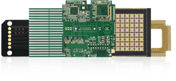
PCB Manufacturing vs Assembly: What Does the Process Really Include?
PCB manufacturing is often used loosely to describe everything from bare board fabrication to fully assembled products. The distinction matters when you request quotes, because you are buying two different services.
PCB fabrication produces the bare board: the laminate, copper traces, vias, solder mask, and surface finish, with no components attached. PCB assembly (PCBA) takes that bare board and populates it with components through solder paste printing, pick-and-place, and reflow or wave soldering. Many PCB manufacturing services offer both under one roof, which is usually called turnkey or one-stop manufacturing.
This guide focuses on fabrication, since that is where the term "PCB manufacturing process" applies most precisely. For a detailed look at the assembly stage, you can read our comprehensive guide to PCB assembly.
The PCB Manufacturing Process: Step by Step
The sequence below reflects how a modern fabrication line builds a multilayer board. Two-layer boards skip the inner layer and lamination stages and move straight from material cutting to drilling.
Step 1: Engineering Review and CAM Processing
Before production begins, engineers review your PCB design files to make sure they can be manufactured reliably. Using Gerber, ODB++, or IPC-2581 files, CAM engineers check key details such as trace width, spacing, drill clearances, solder mask openings, and other manufacturing requirements through a design for manufacturability (DFM) review.
If any issue could affect production quality or yield, the manufacturer will send an engineering query (EQ) for confirmation. To reduce delays and avoid unnecessary revisions, it is important to choose a PCB manufacturer with strong DFM capabilities, such as PCBgogo, which provides free DFM checks to identify potential manufacturing issues before production begins.
After the design passes review, CAM software converts the files into production data, including layer imaging files, drill programs, solder mask and silkscreen data, routing paths, and electrical test information. The PCB design is also arranged into production panels at this stage.
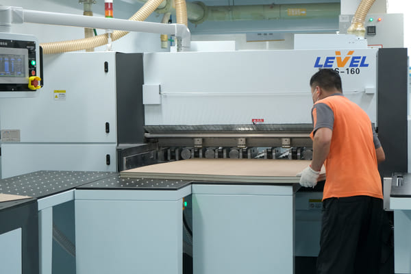
Step 2: Material Cutting
Copper-clad laminate, most commonly FR-4 (a flame-retardant epoxy glass composite), is cut from large sheets into working panels. The laminate grade is chosen based on your specification: standard Tg 135 to 140 material for general products, high-Tg (170+) for boards that see lead-free reflow multiple times or elevated operating temperatures, and specialty laminates like polyimide or PTFE-based materials for flex and RF applications.
Step 3: Inner Layer Imaging
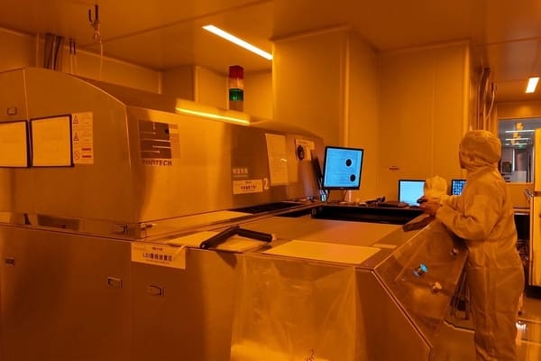
Each inner layer core gets a coat of photoresist, a light-sensitive film. The circuit pattern is then transferred onto it. Modern fabs use laser direct imaging (LDI), where a computer-controlled laser writes the pattern straight from the CAM data onto the resist, eliminating the photo film (artwork) used in older lines. LDI holds registration accuracy that film-based exposure cannot match, which is why it has become the default for fine-pitch and HDI work.
After exposure, a developer solution washes away the unexposed resist, leaving hardened resist exactly where copper should remain.
Step 4: Inner Layer Etching and Resist Stripping
The panel passes through a conveyorized etch line where an etchant chemically removes all copper not protected by resist. Etch quality depends on tight control of chemistry concentration, conveyor speed, and spray pressure. Poor control produces under-etch (shorts between traces) or over-etch (thinned traces that fail current or impedance requirements).
The remaining resist is then stripped off, revealing the finished inner layer circuitry.
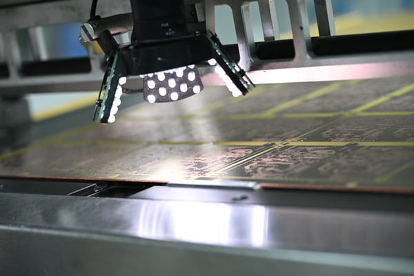
Step 5: Automated Optical Inspection (AOI) of Inner Layers
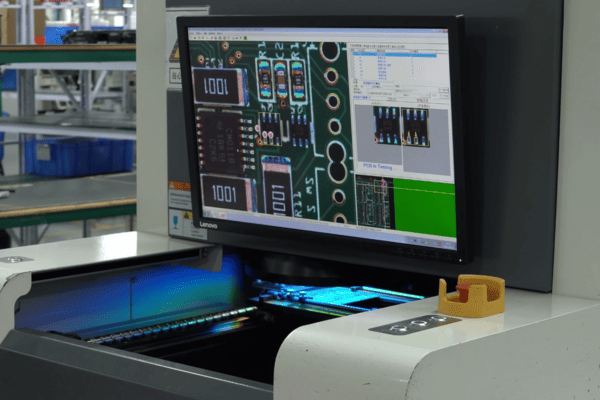
Every inner layer is scanned by an AOI system that compares the etched pattern against the original CAM data, pixel by pixel. This step exists because inner layer defects become unreachable after lamination. A short or open caught here costs one core; caught after lamination, it scraps the entire panel.
Step 6: Oxide Treatment and Lay-Up
Inner layer copper surfaces receive an oxide (or oxide alternative) treatment that micro-roughens the copper to improve bonding with prepreg resin. The layers are then stacked in the specified order: core, prepreg sheets, copper foil, repeated per your stackup design, with the whole book aligned on registration pins.
Step 7: Lamination
The stacked book goes into a heated hydraulic press. Under controlled temperature, pressure, and vacuum, the prepreg resin flows, fills the etched circuitry, and cures, bonding everything into a single solid board. Press cycles are material-specific; high-Tg and low-loss laminates cure at different profiles than standard FR-4.
Lamination is also where layer-to-layer registration is won or lost. Material shrinks slightly as it cures, and good fabricators apply predictive scaling factors to the inner layer artwork to compensate.
Step 8: Drilling
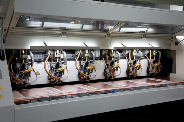
Computer-controlled drill machines bore every through-hole and via, using X-ray systems to locate inner layer targets and align the drill program. Mechanical drilling handles holes down to about 0.15 to 0.2 mm; smaller microvias in HDI boards are drilled by laser (covered in the HDI section below).
Drilling generates heat, and heat smears epoxy resin across the inner layer copper exposed inside the hole barrel. That smear must be removed before plating, or the via will fail to connect the layers.
Step 9: Desmear and Electroless Copper Deposition
A chemical desmear process (permanganate or plasma) cleans resin smear from the hole walls. The panel then goes through electroless copper deposition, an autocatalytic chemical bath that deposits a thin, uniform copper seed layer over the entire panel surface and, critically, inside every hole barrel. This seed layer, typically under a micron thick, is what makes the non-conductive hole walls platable.
Step 10: Outer Layer Imaging and Pattern Plating
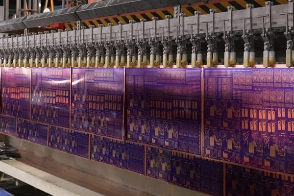
Outer layers are imaged the same way as inner layers, but with a reversed logic: resist covers the areas that will be etched away, leaving the future circuitry exposed. The panel is then electroplated, building copper up to the specified thickness on the exposed traces and inside the hole barrels. IPC-6012 Class 2 requires an average of 20 microns (about 0.8 mil) of plated copper in the hole wall; Class 3 requires 25 microns.
A thin layer of tin is plated on top of the copper as an etch resist for the next step.
Step 11: Outer Layer Etching and Tin Stripping
The plating resist is stripped, exposing the unwanted background copper, which is etched away. The tin layer protects the plated circuitry during this etch. The tin is then stripped off, leaving the finished outer layer copper pattern.
Step 12: Solder Mask Application
Liquid photoimageable (LPI) solder mask is coated over both sides of the panel, exposed with the mask artwork, developed to open the pads and holes that must stay solderable, and thermally cured. Solder mask does three jobs: it insulates adjacent traces, defines solderable areas during assembly, and protects the copper from oxidation and handling damage.
Green remains the most common color for a practical reason: green mask offers the best-characterized imaging resolution and inspection contrast on most production lines, though black, blue, red, and white are all standard options now.
Step 13: Surface Finish
Exposed copper pads oxidize quickly, so a surface finish is applied to preserve solderability. The choice affects assembly yield, shelf life, and cost:
| Finish | Flatness | Shelf Life | Typical Use Case | Relative Cost |
|---|---|---|---|---|
| HASL / Lead-free HASL | Poor to fair | 12+ months | General-purpose boards and larger pitch components | Lowest |
| OSP | Excellent | 6 months | Cost-sensitive, high-volume consumer electronics | Low |
| Immersion Tin | Excellent | 6 months | Press-fit connectors and fine-pitch components | Medium |
| Immersion Silver | Excellent | 6 to 12 months | RF and high-frequency circuit boards | Medium |
| ENIG | Excellent | 12+ months | Fine-pitch BGA, mixed assembly, and reliable general-purpose applications | High |
| ENEPIG | Excellent | 12+ months | Applications requiring both wire bonding and soldering on the same PCB | Highest |
If your board carries fine-pitch BGAs or 0402 and smaller passives, HASL's uneven surface becomes an assembly risk, and a flat finish like ENIG is worth the premium. Edge connectors and other high-wear contact areas are the exception; those typically call for hard gold plating applied selectively over the contact fingers.
Step 14: Silkscreen (Legend Printing)
Reference designators, polarity marks, logos, and part numbers are printed onto the mask surface, today mostly by direct inkjet legend printers driven straight from the CAM data.
Step 15: Electrical Test
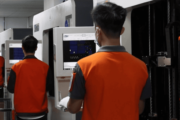
Every net on the board is tested for opens and shorts against the IPC netlist generated back in Step 1. Two methods dominate: flying probe testing, where moving probe heads touch each test point in sequence (no fixture cost, ideal for prototypes and small batches), and fixture-based bed-of-nails testing, which tests all nets simultaneously (faster per board, economical only at volume once the fixture is built).
Step 16: Profiling, Final Inspection, and Packing
Individual boards are cut from the panel by CNC routing (leaving breakaway tabs) or V-scoring (cutting partial-depth grooves for snap-apart panels). Final inspection verifies dimensions, hole sizes, mask registration, and cosmetic criteria against IPC-A-600 acceptance standards. Boards are then vacuum-packed with desiccant to protect the surface finish during transit and storage.
How the Process Changes for Multilayer PCB Manufacturing
The step sequence above describes a standard multilayer build, but layer count changes more than just the number of cores in the lay-up. Three things scale with complexity:
Registration budget shrinks. A 4-layer board has one lamination cycle and two drilled interfaces to align. A 12-layer board stacks up alignment tolerance across five cores, and every layer pair must land within the annular ring budget. This is why fabricators publish tighter minimum annular ring requirements as layer counts rise, and why X-ray drilling and post-etch punch systems matter more on high layer count work.
Impedance control becomes a manufacturing spec, not just a design spec. Multilayer boards carrying high-speed signals specify controlled impedance, usually with a plus or minus 10 percent tolerance (7 to 8 percent at advanced fabs). Hitting it requires the fab to control dielectric thickness after resin flow, trace width after etch, and copper thickness after plating simultaneously. Ask any prospective fabricator whether they verify impedance with test coupons on every panel; the good ones do, and can share coupon TDR reports.
Material choices interact with the press cycle. Mixing standard FR-4 cores with low-loss laminates in one stackup is possible but requires a press profile that satisfies both resins. Fabricators with real multilayer PCB manufacturing depth will review your stackup and propose adjustments rather than silently building a marginal one.
HDI PCB Manufacturing: Sequential Lamination and Microvias
High density interconnect (HDI) boards break the standard flow in a fundamental way: they are built through sequential lamination, where the board is laminated, laser-drilled, and plated multiple times, adding one build-up layer pair per cycle.
The defining features:
Laser-drilled microvias. A CO2 or UV laser ablates vias typically 0.075 to 0.15 mm in diameter, far below mechanical drilling limits. Microvias connect only adjacent layers, which frees routing space and enables via-in-pad designs under fine-pitch BGAs.
Via structures by build-up count. HDI stackups are described in the form 1+N+1, 2+N+2, and so on, where the outer numbers are build-up layers with microvias and N is the laminated core. Each additional build-up cycle adds a full lamination, drilling, and plating pass, so a 2+N+2 board costs meaningfully more than a 1+N+1, independent of layer count.
Via filling. Microvias placed in pads must be filled (copper-filled or resin-plugged and capped) to present a flat, solderable surface. Copper-filled vias also improve thermal paths under hot components.
Stacked vs. staggered microvias. Stacking microvias directly on top of each other saves the most routing space but is the most demanding structure to plate reliably. IPC and industry reliability studies have pushed many design teams toward staggered microvias for high-reliability products. If your design stacks microvias, verify that the fabricator performs reflow simulation or thermal shock testing on stacked via coupons.
Prototype PCB Manufacturing vs. Mass Production
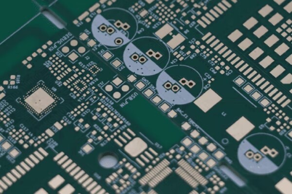
Prototype and volume PCB manufacturing use similar processes, but the priorities are different. Understanding these differences helps you choose the right manufacturing approach for each stage of your project.
Prototype PCB manufacturing focuses on speed and flexibility. Small runs (typically 5–50 boards) use standardized materials, shared panels, and methods such as flying probe testing to reduce setup time. Because tooling and setup costs are spread across fewer boards, the unit price is usually higher.
Volume production focuses on consistency, efficiency, and lower cost per board. Manufacturers use dedicated panels, production fixtures, process controls, and full traceability systems to maintain stable quality across large quantities. Although production takes longer, the cost per unit decreases significantly.
For a more detailed comparison of prototype and mass production PCB manufacturing, see our complete guide to prototype PCB vs. mass production.
Reading a PCB Fabrication Capabilities Sheet
Every serious fabricator publishes a capabilities table. Most engineers skim it. Reading it carefully tells you whether your design lands in the fab's comfortable center or at its bleeding edge, which directly predicts yield, price, and how often you will hear from their EQ department.
| Parameter | Mainstream Capability | Advanced Capability | Why It Matters |
|---|---|---|---|
| Layer count | 1 to 14 layers | 16 to 32+ layers | Higher layer counts require tighter layer registration and more precise control of thicker PCB panels |
| Min trace/space | 4/4 mil (0.10 mm) | 2.5/2.5 mil or below | Below 4 mil, manufacturing costs increase due to tighter tolerances and lower yield margins |
| Min mechanical drill | 0.20 mm | 0.15 mm | Smaller drill sizes wear tools faster and increase fabrication costs |
| Min laser microvia | 0.10 mm | 0.075 mm | Required for advanced HDI PCB designs with high-density interconnects |
| Max aspect ratio (through-hole) | 8:1 | 12:1 or higher | Higher aspect ratios make hole-wall plating more difficult and require better process control |
| Copper weight | 0.5 to 2 oz | 3 to 12 oz (heavy copper) | Heavy copper affects etching, plating, thermal performance, and lamination processes |
| Impedance tolerance | ±10% | ±7% | High-speed interfaces may require tighter impedance control for signal integrity |
| Board thickness | 0.4 to 2.4 mm | 0.2 to 6.0 mm | Very thin or thick PCBs require specialized manufacturing and handling processes |
Three reading tips that capability sheets never state outright. First, the published minimum is not the recommended value; designing at the minimum trace/space means every panel flirts with the etch tolerance limit. Give yourself margin wherever the layout allows. Second, parameters interact: a fab may support 0.15 mm drills and 2.4 mm thickness separately but not together, because the combination exceeds their aspect ratio limit. Third, capabilities for prototypes and volume production sometimes differ at the same company; confirm which table applies to your order type.
Quality Standards and Testing in PCB Manufacturing
Quality claims are cheap. Standards compliance is checkable. These are the references that matter when evaluating PCB manufacturing services:
IPC-A-600 defines the visual acceptance criteria for finished boards: what counts as an acceptable void, nick, or mask misregistration, and what constitutes a reject. IPC-6012 defines the qualification and performance requirements, split into classes: Class 2 for general electronic products (the default for most commercial work) and Class 3 for high-reliability products where failure is not tolerable, with tighter requirements on plating thickness, annular ring, and etch quality.
Beyond the standards themselves, the testing regime tells you how a factory actually catches defects:
In-process AOI on every inner layer catches shorts and opens before they get buried. 100 percent electrical test against the IPC netlist verifies connectivity on every shipped board; confirm this is standard rather than an option. Microsection (cross-section) analysis cuts a coupon from the panel and examines hole-wall copper thickness, plating integrity, and lamination quality under a microscope, and is the definitive check on via reliability. Impedance coupon testing with a TDR verifies controlled impedance panels. Solderability and thermal stress testing confirm the surface finish will survive assembly.
When you audit or evaluate a fabricator, ask for a sample first article report. A factory operating under real IPC-6012 discipline can produce microsection photos, impedance coupon data, and e-test records for any recent lot without scrambling.
How to Choose a PCB Manufacturing Company
The selection question behind many "pcb manufacturing" searches deserves a direct answer. Evaluate candidates on five checkable dimensions:
1. Capability match, with margin. Compare your design's toughest parameters (finest trace/space, smallest drill, highest aspect ratio, impedance tolerance) against the fab's published capabilities. You want your design in their mainstream band, not at their advertised limit.
2. Verifiable quality system. Look for IPC-A-600 inspection practice, IPC-6012 Class 2 or 3 build capability, AOI on inner layers, and 100 percent electrical test as standard. Certifications like ISO 9001 are table stakes; the ability to produce microsection and coupon reports on request is the stronger signal.
3. Engineering support before the order. A fabricator that runs a genuine DFM review and raises engineering queries before production is protecting your yield. One that accepts any file without question is transferring the risk to you.
4. Quoting transparency and speed. Instant online quoting with visible price breakdowns by spec lets you run cost trade-offs (layer count, finish, quantity, lead time) yourself in minutes, which is far more useful than emailing a sales inbox and waiting two days per iteration.
5. Scalability across order sizes. If your product will move from prototype to production, confirm the manufacturer handles both under consistent process rules, and ask how engineering data, stackups, and impedance models carry over between order types.
Applying that checklist in practice: for teams that want one platform covering the full range, PCBgogo checks these boxes with a one-stop service spanning PCB prototyping, multilayer fabrication, small-batch and volume production, and SMT assembly, built to IPC-A-600 and IPC-6012 acceptance criteria with AOI inspection and free DFM review on incoming designs. Its online self-service quoting system returns real-time pricing across spec options, which makes the cost trade-off exercise described above genuinely fast, and its manufacturing base has served customers in more than 200 countries and regions since 2013. It is a sensible shortlist candidate whether you are ordering five prototype boards this week or planning the batch run behind them.
FAQ: PCB Manufacturing
How long does PCB manufacturing take?
Standard 2-layer prototypes ship in 24 to 48 hours at quick-turn fabs. Standard 4 to 8 layer boards typically take 3 to 7 days. HDI, heavy copper, and high layer count boards run 1 to 3 weeks depending on build-up cycles. Volume production orders generally quote 2 to 4 weeks. Assembly adds 3 to 10 days on top of fabrication depending on component availability.
What is the difference between PCB fabrication and PCB manufacturing?
In strict usage, fabrication means producing the bare board, while manufacturing is often used as an umbrella term that can include assembly. In practice the terms are used interchangeably for bare board production. When requesting quotes, specify explicitly whether you need bare boards only or fabrication plus assembly (turnkey PCBA).
What files does a PCB manufacturer need?
Gerber files (RS-274X) or ODB++ or IPC-2581 for the layer images, an NC drill file, and a fabrication drawing or notes specifying material, thickness, copper weight, solder mask and legend colors, surface finish, and any impedance requirements. For assembly, add the BOM, centroid (pick-and-place) file, and assembly drawings.
What is the minimum trace width in PCB manufacturing?
Mainstream fabrication reliably supports 4 mil (0.10 mm) trace and space. Advanced processes reach 2.5 mil and below, and specialized mSAP processes go finer still. Designing at 5 to 6 mil where layout allows improves yield and cost on any process.
How many layers can a PCB have?
Common commercial boards run 2 to 16 layers. Advanced fabricators routinely build 20 to 32 layers, and specialized backplane and test equipment boards exceed 60. Layer count is bounded in practice by registration tolerance, drilling aspect ratio, and cost rather than any hard physical limit.
Is HDI PCB manufacturing more expensive than standard multilayer?
Yes, primarily because each HDI build-up layer pair adds a full sequential lamination, laser drilling, and plating cycle. A 1+N+1 build typically adds 30 to 50 percent over a comparable standard multilayer; 2+N+2 adds more. HDI often pays for itself at the system level, though, by cutting layer count or board size that standard through-hole via routing would require.
References
1. IPC-A-600, Acceptability of Printed Boards, IPC International.
2. IPC-6012, Qualification and Performance Specification for Rigid Printed Boards, IPC International.
3. IPC-2581, Generic Requirements for Printed Board Assembly Products Manufacturing Description Data, IPC International.
4. IPC-4101, Specification for Base Materials for Rigid and Multilayer Printed Boards, IPC International.
5. IPC-2226, Sectional Design Standard for High Density Interconnect (HDI) Printed Boards, IPC International.





