



 日本語
日本語
 한국어
한국어

HDI PCB Manufacturing Service: Benefits, Applications, and Design Considerations
Electronic devices keep getting smaller, faster, and more powerful, and the printed circuit boards inside them have had to keep pace. High-Density Interconnect (HDI) technology is the reason a modern smartphone motherboard can pack in more routing, more components, and more functionality than boards many times its size just a decade ago. If your next project demands finer traces, smaller vias, and tighter component spacing, working with an experienced provider of HDI PCB manufacturing services is essential to getting a reliable, high-yield board. This article covers what HDI PCBs are, their key benefits, where they're used, and the design considerations engineers should keep in mind before sending files out for fabrication.
What is an HDI PCB, and how is it built differently from a standard board?
An HDI PCB is a circuit board that packs more routing into less board area by replacing most through-hole vias with laser-drilled microvias — typically under 150 microns (0.15mm) in diameter — combined with finer traces and stacked or staggered via structures. That's the one-sentence version. The reason it needs a different manufacturing process comes down to how those microvias actually get made.
Standard multilayer boards drill straight through the stack with mechanical bits, which limits how small a via can realistically get — usually not much below 0.2mm (8 mil) without reliability problems. HDI fabrication uses laser drilling instead, builds the board in sequential lamination cycles, and inspects each layer pair before adding the next. That's why HDI costs more per square inch: you're paying for laser precision and multiple lamination passes, not just extra copper layers.
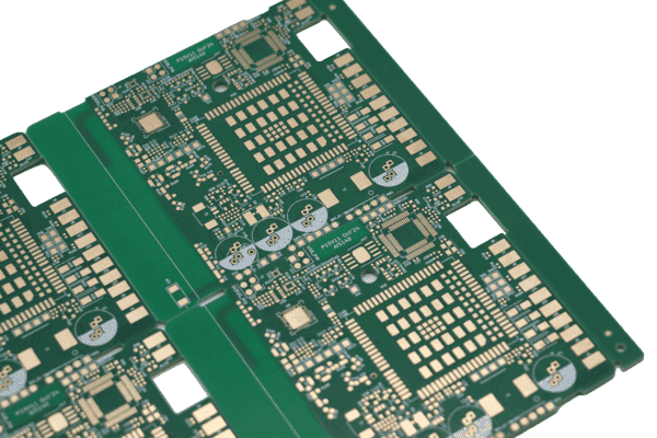
Key Benefits of HDI PCB Technology
1. Significant Miniaturization
Microvias and fine-pitch traces let designers shrink board size dramatically while keeping — or even increasing — functionality. This is why HDI is the default construction method for smartphones, wearables, and other compact consumer electronics.
2. Improved Electrical Performance
Shorter signal paths and smaller vias reduce parasitic inductance and capacitance, which lowers signal loss and improves signal integrity at high frequencies. This makes HDI boards well suited to high-speed digital designs, RF circuits, and applications with strict timing requirements.
3. Higher Reliability
Because HDI boards typically need fewer drilled holes and less mechanical stress on the laminate, they can offer better reliability in demanding thermal and vibration environments when manufactured to tight process control — something a quality-focused HDI PCB manufacturing service should be able to demonstrate with IPC-standard testing and inspection data.
4. Support for Advanced Component Packaging
Fine-pitch BGAs, chip-scale packages (CSPs), and other advanced components require tighter routing than standard PCB technology allows. HDI's microvia and fine-line capabilities make it possible to break out these packages without excessive layer counts.
5. Reduced Layer Count and Overall Weight
By packing more routing into fewer layers, HDI designs often end up thinner and lighter than an equivalent multilayer conventional board — a major advantage for portable and aerospace electronics where every gram counts.
Why designers move to HDI when standard multilayer boards run out of room
Here's the real trigger point: once you're routing a BGA with 0.4mm pitch or tighter, standard vias physically can't fit between the pads anymore. A mechanically drilled via with its annular ring simply eats too much space. So what actually happens? Signal traces either have to route around, which adds layers and length, or the design stalls.
Microvias solve this because they sit directly in the pad (via-in-pad) or tuck into the space a standard via can't reach. That's what lets a smartphone mainboard cram 10+ layers of routing into a footprint smaller than a credit card, or lets a wearable's flex-rigid HDI stack handle a processor, RF module, and power management on one board no bigger than a coin. The tradeoff is real, though — denser routing means tighter tolerances everywhere else too: impedance control, thermal management, and via reliability all get harder to manage as things shrink.
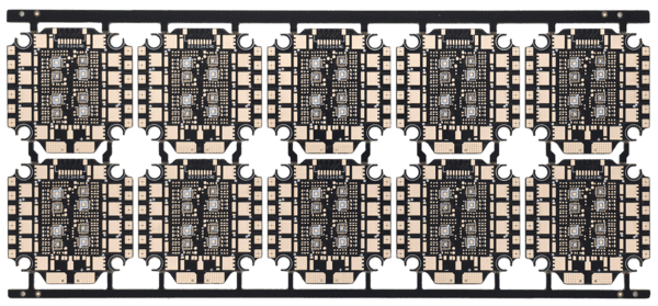
Common Applications of HDI PCBs
Smartphones, tablets, and wearable devices
Medical devices, including implantables and diagnostic equipment
Automotive electronics such as ADAS modules and infotainment systems
Aerospace and defense systems requiring lightweight, high-reliability boards
5G infrastructure and high-speed networking equipment
IoT devices and other compact, battery-powered electronics
Standard multilayer vs. HDI: what's actually different
| Property | Standard Multilayer PCB | HDI PCB |
|---|---|---|
| Via type | Mechanically drilled through-hole vias | Laser-drilled microvias, blind vias, and buried vias |
| Typical min via diameter | ~0.2mm (8 mil) | 0.1mm (4 mil) or smaller |
| Lamination process | Single press cycle | Sequential build-up with multiple lamination cycles |
| Fine-pitch BGA support | Limited capability below 0.5mm pitch | Supports 0.4mm pitch and tighter fine-pitch BGA packages |
| Relative cost | Lower manufacturing cost | Higher cost depending on build-up structure and layer complexity |
Microvia structures you need to understand before specifying HDI
Not all HDI is the same HDI. The build-up structure is usually described by how many laser-drilled layers sit on either side of the core, written as a ratio like 1+N+2.
| Structure | Description | Typical Use |
|---|---|---|
| 1+N+1 | One build-up layer on each side of the core with a single lamination process | Mobile devices and compact consumer electronics |
| 2+N+2 | Two build-up layers on each side with stacked or staggered microvias for higher routing density | High-density networking equipment and RF modules |
| Any-layer HDI | Microvias are available on every layer and can be stacked throughout the entire PCB structure | Advanced smartphone mainboards and high-end server systems |
Stacked microvias route straight down through the build-up, which saves space but concentrates thermal and mechanical stress in one spot. Staggered microvias offset each layer's via location, which is more reliable under thermal cycling but eats more routing area. IPC-2226 lays out the design classes for these structures — if your fabricator can't tell you which class they're building to, that's worth asking about before you commit a design.
Design Considerations for HDI PCBs
1. Stack-Up Planning
Decide early whether the design needs a simple 1+N+1 build-up or a more complex any-layer structure. Layer count, impedance requirements, and via structure all influence cost and manufacturability, so it's worth reviewing stack-up options with your manufacturer before finalizing the schematic.
2. Microvia Types and Via-in-Pad
Choose between stacked, staggered, and skip vias based on routing density and reliability needs. Via-in-pad designs, common with fine-pitch BGAs, typically require via filling and capping to maintain a flat, plateable surface — a process that should be confirmed as part of your fabricator's capabilities.
3. Trace Width and Spacing
HDI boards commonly use trace widths and spacing in the 3-4 mil range or finer. Confirm your manufacturer's minimum feature size and its impact on yield, since pushing below a fabricator's proven process window can increase defects and cost.
4. Material Selection
High-speed designs may need low-loss laminates, while boards with tight thermal requirements may call for materials with better thermal conductivity or a higher glass transition temperature (Tg). Material choice should be matched to the electrical and mechanical demands of the end application.
5. DFM and Testing
Because HDI processes are less forgiving of design errors than conventional PCB fabrication, a thorough design-for-manufacturability (DFM) check before production is critical. Look for a manufacturing partner that offers DFM feedback, AOI (automated optical inspection), and electrical testing as standard parts of the HDI PCB manufacturing service.
Why Choose PCBgogo for HDI PCB Manufacturing Services
Getting HDI right requires tight process control, modern laser-drilling and plating equipment, and engineers who understand the trade-offs between density, yield, and cost. PCBgogo provides HDI PCB manufacturing services built around exactly that combination, offering:
Support for advanced stack-ups, including 1+N+1, 2+N+2, and any-layer builds
Fine-line and microvia capabilities suited to fine-pitch BGA and CSP designs
Free DFM review to catch manufacturability issues before production
A broad range of laminate options for high-speed, high-thermal, and general-purpose applications
AOI, electrical testing, and quality documentation on every order
Fast turnaround options, from prototype quantities to volume production
Responsive engineering support for questions on stack-up, via structure, or material selection
Whether you're developing a compact wearable, a high-speed networking board, or a mission-critical medical device, PCBgogo's HDI PCB manufacturing services are built to help you move from design to reliable, tested hardware with confidence.
Get an HDI PCB Quote
Ready to move forward with your HDI design? Upload your Gerber files to PCBgogo for a fast quote and a free DFM check, or reach out to PCBgogo's engineering team with questions about stack-up planning, microvia structures, or material selection for your next HDI PCB project.
Common questions about HDI PCB manufacturing
Q: What's the minimum via size a manufacturer needs to support for real HDI work?
A: Look for laser-drilled microvia capability at 0.1mm (4 mil) diameter or smaller. If a shop's minimum sits at 0.15mm or above, they're offering "HDI-adjacent" capability, not true fine-pitch HDI.
Q: How many build-up layers (1+N+1 vs. 2+N+2) do I actually need?
A: If your densest component is a single 0.4mm-pitch BGA, 1+N+1 is usually enough. Multiple fine-pitch parts or RF sections routing on several layers typically push you to 2+N+2 or any-layer HDI — going higher than your design actually needs just adds cost and lamination cycles for no routing benefit.
Q: Is HDI worth it for a low-volume prototype run?
A: If the design genuinely requires fine-pitch routing that a standard board can't achieve, yes — there's no way around it regardless of volume. If HDI is being considered purely to shrink board size on a design that could still route on a standard multilayer board, prototype on the standard board first and reserve HDI for the production form factor.





