



 日本語
日本語
 한국어
한국어

HDI PCB Overview: Design Basics, Advantages & Common Electronic Uses
QUICK ANSWER An HDI PCB (High Density Interconnect PCB) is a printed circuit board that uses microvias, blind vias, and buried vias combined with fine-line routing to achieve extremely high connection density in a compact area. Defined under IPC-2226, HDI designs typically use microvias no larger than about 150 micrometers, enabling designers to reduce layer count, shrink board size, and support fine-pitch BGAs while maintaining short, high-performance signal paths.
Try fitting a modern smartphone's circuitry onto a board built with 1990s through-hole technology and you would end up with something the size of a laptop. High Density Interconnect PCBs are the reason that did not happen. By replacing bulky through-hole vias with microscopic laser-drilled connections, HDI technology lets engineers pack more signal paths into less board area than a standard multilayer PCB ever could.
This guide covers what makes an HDI PCB different from a standard board, the stack-up types you will encounter, how these boards get manufactured, and what to look for in a supplier to help you select suitable HDI PCB solutions smoothly.
What Is an HDI PCB?
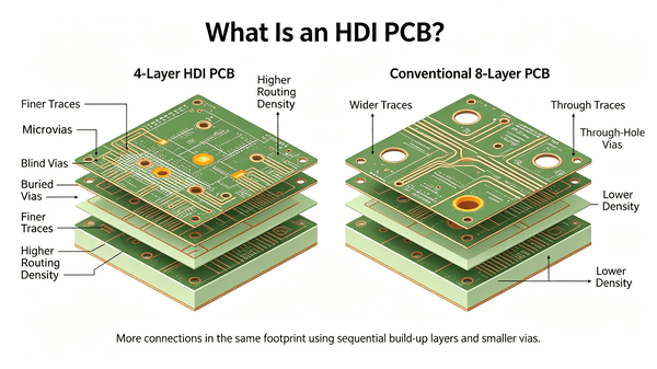
An HDI PCB is a printed circuit board built with a higher wiring density per unit area than a standard multilayer board, achieved through microvias, blind vias, and buried vias instead of full-depth through-hole connections. These smaller vias, combined with trace widths often below 3 mils, let designers route far more connections into the same footprint.
HDI construction typically pairs a standard core layer with one or more build-up layers added through sequential lamination. A board that would need 8 layers using conventional through-hole vias can often be redesigned as a 4-layer HDI board with the same electrical functionality, since each HDI layer carries more routing density than its conventional counterpart. This is why HDI has become the default choice for compact, high-pin-count designs like smartphone mainboards and fine-pitch BGA modules.
HDI PCB vs Standard PCB: Key Differences
A standard PCB relies on mechanically drilled through-hole vias that run the full thickness of the board, which limits how tightly components and traces can be packed. HDI boards solve that constraint with microvias that connect only the layers that need to communicate, freeing up space everywhere else.
The table below summarizes the core differences between the two approaches.
| Attribute | Standard PCB | HDI PCB |
|---|---|---|
| Via type | Through-hole, mechanically drilled | Microvias, blind vias, buried vias |
| Typical via diameter | 0.15–0.20 mm | 0.05–0.15 mm (laser drilled) |
| Trace width/spacing | Often ≥ 4 mils | Frequently < 3 mils |
| Aspect ratio | Can exceed 10:1 for deep through-holes | Typically ~1:1 for microvias |
| Best suited for | Lower frequency, larger, cost-sensitive designs | Fine-pitch BGAs, high-speed signals, compact devices |
Once you understand this structural difference, the stack-up terminology used to classify HDI boards starts to make a lot more sense.
HDI PCB Types and Stack-Up Classifications
HDI stack-ups are classified under IPC-2226 based on how many build-up layers surround the core and how the microvias are arranged. Each type trades manufacturing complexity for routing density.
Type I (1+N+1): A single microvia layer sits on each side of a standard core, with no via stacking. This is the simplest and most cost-effective HDI configuration, suited to moderately dense consumer designs.
Type II (2+N+2): Two build-up layers sit on each side of the core, incorporating microvias, blind vias, and buried vias together. This configuration offers higher routing density than Type I while remaining manufacturable at reasonable cost.
Type III (2+N+2 or more): Two or more microvia layers are built up on each side of the core, often with stacked or staggered microvias connecting through multiple layers. This is the configuration typically chosen for high-speed, high-reliability designs like servers and advanced networking hardware.
Type IV through VI: These represent the most advanced stack-ups, including coreless (any-layer) construction and embedded passive components. They deliver maximum density but come with the highest manufacturing cost and longest lead times.
Understanding which type a design calls for is the first step toward evaluating whether the benefits are worth the added process complexity.
Key Benefits of HDI PCB Technology
The appeal of HDI comes down to doing more with less board space, without giving up signal performance.
Smaller board footprint: Because HDI layers carry more routing density, an 8-layer standard PCB can frequently be replaced by a 4-layer HDI board with equivalent functionality, cutting overall size and weight substantially.
Shorter signal paths: Microvias connect only adjacent layers instead of running the full board thickness, which shortens signal travel distance and reduces transmission delay, a meaningful advantage for high-speed interfaces like DDR4, PCIe, and USB 3.0.
Improved reliability under thermal stress: Microvias typically have an aspect ratio around 1:1, compared to much deeper through-hole vias, making them less prone to cracking during thermal cycling in automotive or aerospace environments.
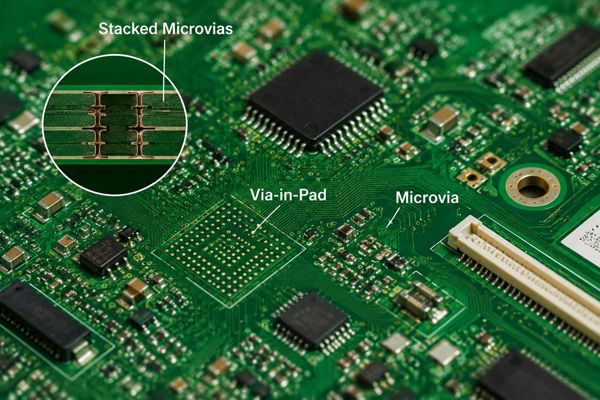
Support for fine-pitch components: Via-in-pad techniques let designers place microvias directly inside BGA pads, which is often required for packages with a pitch below 0.5 mm.
Better long-term cost efficiency: Fewer layers and smaller boards can offset the higher per-layer manufacturing cost of HDI, particularly in high-volume production runs.
These benefits are only achievable, though, if the manufacturing process behind them is dialed in correctly.
How HDI PCBs Are Manufactured
HDI manufacturing follows a sequential build-up (SBU) process, adding layers to the core one step at a time rather than laminating the whole stack at once.
1. Core lamination: Start with a standard double-sided or multilayer core, plated and etched like a conventional PCB.
2. Build-up layer lamination: Bond a prepreg and copper foil layer onto each side of the core under heat and pressure.
3. Laser drilling: Drill microvias through the new layer down to the copper below. CO2 lasers handle 100 to 150 micrometer holes; UV lasers handle 25 to 80 micrometer holes with less thermal damage.
4. Desmear and plating: Clean drilling residue from the via walls, then plate the microvia with copper to form the electrical connection.
5. Via filling: Fill stacked microvias with electroplated copper for mechanical support and reliable interlayer connection.
6. Repeat for additional layers: Type II and Type III boards repeat steps 2 through 5 for each additional build-up layer.
7. Outer layer processing: Image and etch the outer circuitry, then apply solder mask, surface finish, and silkscreen.
Aspect ratio control (hole depth to diameter, generally kept at or below 10:1) is critical throughout this process and directly affects plating reliability.
Getting an HDI design right depends on the fabricator's process control just as much as the layout itself. PCBgogo runs laser drilling, sequential lamination, and automated optical inspection in house, so tight aspect ratios and fine line spacing hold up from prototype through volume production, without sacrificing turnaround time. If you are planning an HDI build and want a second set of eyes on your stack-up before it goes to fabrication, PCBgogo's engineering team is a good place to start that conversation.
Common Applications of HDI PCB Technology
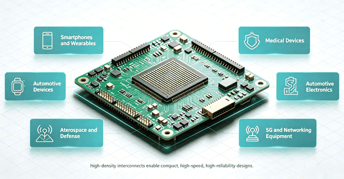
HDI boards show up anywhere a device needs to be smaller, lighter, or faster without losing functionality.
Smartphones and wearables: High pin-count processors and fine-pitch BGAs make HDI the default choice for mainboards in phones, smartwatches, and other compact consumer electronics.
Medical devices: Implantable devices like pacemakers, along with miniaturized imaging and diagnostic equipment, rely on HDI's small footprint to fit dense electronics into constrained spaces.
Automotive electronics: Radar modules, ADAS systems, and infotainment units use HDI boards to withstand the thermal cycling common in vehicle environments while supporting high-speed data links.
Aerospace and defense: Weight and space constraints make HDI attractive for avionics and communication systems, where the lower aspect ratio of microvias also improves reliability under vibration and temperature extremes.
5G and networking equipment: High-speed signal requirements in 5G infrastructure and data networking hardware benefit from the shorter signal paths that HDI stack-ups provide.
Choosing an HDI PCB Board Supplier
Not every PCB manufacturer offers full HDI capability. Before you send over a design, it's worth confirming a few key details. Ask if the supplier does laser drilling in house, rather than outsourcing it. This affects both lead time and quality control over microvia formation. Also confirm their aspect ratio limits and minimum microvia diameter. These numbers determine whether your stack-up is actually manufacturable. And ask about their experience with the specific stack-up type your design needs. A supplier who's great at Type I builds may not be ready for Type III designs with stacked microvias. Finding that out early saves a lot of rework later.
PCBgogo's HDI process is built around these exact concerns. We keep tight control over microvia quality. We choose materials that meet the tight tolerances HDI stack-ups demand. And our engineering team has real hands-on experience with Type I, II, and III builds, including stacked and staggered microvias. If you're planning an HDI project, reach out to our team. We'll go over your stack-up together and help you get your project done smoothly and efficiently.
Conclusion
HDI PCB technology solves a straightforward problem: modern devices need more connections in less space, and microvias make that possible without sacrificing signal integrity. The right stack-up choice, whether Type I or Type III, comes down to matching design complexity with a fabricator that has genuine HDI process experience. When you are ready to move your HDI design toward production, PCBgogo's team can help review your stack-up and put together a quote.
Frequently Asked Questions
What is the difference between an HDI PCB and a standard PCB?
A standard PCB uses through-hole vias that run the full board thickness and generally has wider traces and lower routing density. An HDI PCB uses microvias, blind vias, and buried vias to connect only the layers that need it, allowing significantly finer traces and higher component density in the same footprint.
What is a microvia in an HDI PCB?
A microvia is a small, laser-drilled hole, typically under 150 micrometers in diameter, that connects two adjacent layers of an HDI board. Unlike through-hole vias, microvias do not need to span the entire board thickness, which saves space and shortens signal paths.
What are the main HDI PCB stack-up types?
IPC-2226 defines HDI stack-ups primarily as Type I (1+N+1, one build-up layer per side), Type II (2+N+2, with blind and buried vias added), and Type III (multiple stacked microvia layers per side). More advanced Type IV through VI configurations use coreless or embedded-component construction.
Are HDI PCBs more expensive than standard PCBs?
HDI boards typically cost more per layer due to laser drilling and sequential lamination, but the reduction in total layer count and board size often narrows or offsets that gap, especially in higher-volume production where fewer layers translate directly into material savings.
What industries use HDI PCB technology?
HDI is common in consumer electronics like smartphones and wearables, medical devices including implantables and diagnostic equipment, automotive radar and ADAS systems, aerospace and defense electronics, and 5G or networking infrastructure where compact size and high-speed performance both matter.





