



 日本語
日本語
 한국어
한국어

Gerber File Format Explained: A Complete Guide to PCB Fabrication Data
If you design printed circuit boards, the Gerber file is the language you use to talk to your fabricator. Get it right, and your board comes back exactly as designed. Get it wrong, and you're looking at CAM holds, re-spins, or a board that simply doesn't work. This guide breaks down what a Gerber file actually contains, how the format evolved, how it compares to alternatives like ODB++ and IPC-2581, and the specific mistakes that most often delay a fabrication run.
What Is a Gerber File?
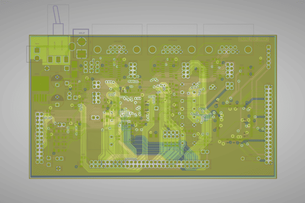
A Gerber file is a 2D vector description of one layer of a PCB design — not the whole board at once. A typical multilayer project therefore ships as a set of Gerber files: one for each copper layer, one for each solder mask, one for silkscreen, one for the board outline, plus separate drill files for plated and non-plated holes. Together, this file set is what a fabrication house loads into its CAM (computer-aided manufacturing) system to prepare tooling, phototools, and machine instructions for every stage of production.
The format is intentionally text-based (ASCII), which means a Gerber file can be opened and inspected in any plain text editor. Inside, you'll find a short header defining units and coordinate format, followed by a stream of drawing commands. Each command tells the plotting or imaging equipment to either draw a line, move without drawing, or flash a shape at a given coordinate — the same logic used since the format's earliest photoplotter days, just applied to modern laser and inkjet imaging systems today.
From RS-274D to Gerber X2: A Brief History
The format takes its name from Joseph Gerber, whose company pioneered the vector photoplotter in the 1960s and published the first Gerber format specification in 1980 as a subset of the EIA RS-274-D standard. That original version — now called Standard Gerber or RS-274D — only recorded coordinates and aperture numbers. The actual shapes those numbers referred to lived in a separate, informally-agreed "aperture" or "wheel" file, which made automated data exchange between designer and fabricator unreliable.
RS-274X (Extended Gerber), released in 1998, solved that problem by embedding aperture definitions directly inside the Gerber file itself, so no external file is needed to interpret it. This made each layer file self-contained and is the reason RS-274X remains the format nearly every fabricator, including PCBgogo, expects today. More recently, Gerber X2 extended RS-274X further by adding attributes that label each file with its function — for example, marking a file as top copper or bottom solder mask — which cuts down on the layer-mix-ups that happen when files are misnamed.
| Standard | Aperture Data | Status Today |
|---|---|---|
| RS-274D (Standard Gerber) | External wheel/aperture file required | Obsolete — avoid for new designs |
| RS-274X (Extended Gerber) | Embedded in the file | Current industry standard |
| Gerber X2 | Embedded, plus function attributes | Recommended where supported |
| GerberJob | N/A — job-level metadata file | Optional companion file for stackup/finish data |
How a Gerber File Is Structured
Every RS-274X file follows the same basic shape: a header block that sets the measurement units (inches or millimeters) and coordinate format, followed by data blocks that generate an ordered stream of graphic objects. Three commands do almost all of the work:
D01 (Draw) — moves to a coordinate with the "pen" down, creating a track, trace, or outline segment.
D02 (Move) — repositions to a coordinate without drawing, used to jump between separate shapes.
D03 (Flash) — stamps a predefined aperture shape at a coordinate, used for pads, vias, and other filled features.
Because apertures behave like fonts — reusable shapes referenced by a code rather than redrawn from scratch — a Gerber file can describe complex pad geometry, including BGA and QFN land patterns, without repeating shape data for every instance. This keeps files compact even for dense, high-pin-count designs.
The Standard Gerber File Set for a PCB Project
A single-layer board might need only three or four files, but a multilayer design requires a distinct file per copper layer plus mask, silkscreen, and drill data. Consistent, unambiguous naming matters just as much as the data itself — a mislabeled inner layer is one of the most common causes of a CAM hold.
| Layer / Data | Typical File Content | Common Extension |
|---|---|---|
| Top / Bottom Copper | Traces, pads, copper pours | .GTL / .GBL |
| Inner Copper Layers | Internal routing and planes | .G1, .G2 ... or .GP1, .GP2 |
| Top / Bottom Solder Mask | Mask openings over copper | .GTS / .GBS |
| Top / Bottom Silkscreen | Legend, reference designators | .GTO / .GBO |
| Board Outline / Keepout | Mechanical profile of the board | .GKO / .GM1 |
| Plated Drill Data (PTH) | Vias and plated component holes | .TXT / .DRL (Excellon) |
| Non-Plated Drill Data (NPTH) | Mounting holes, unplated holes | .TXT / .DRL (Excellon) |
| Netlist (optional) | Electrical connectivity for verification | IPC-D-356A |
Gerber vs. ODB++ vs. IPC-2581: When to Use Which
Gerber isn't the only fabrication data format, and it's worth knowing what the alternatives offer even though Gerber (RS-274X) remains the safest default for most projects.
| Format | File Structure | Best For | Adoption |
|---|---|---|---|
| Gerber (RS-274X / X2) | One file per layer, plus separate drill files | Standard multilayer boards; universal fabricator support | Near-universal |
| ODB++ | Single job archive containing all layers, netlist, and stackup | Complex or high-density designs where a single consolidated dataset reduces mismatch risk | Strong among larger EDA tools and CMs |
| IPC-2581 | Single open XML-based file with layers, netlist, and BOM | Teams wanting a vendor-neutral, fully automated data exchange | Growing, less universal than Gerber |
In practice, most fabrication shops build their workflow around Gerber because it's supported by every major EDA tool and requires no proprietary import step. Unless your contract manufacturer specifically asks for ODB++ or IPC-2581, a clean RS-274X Gerber set with Excellon drill files is the safest and fastest path to production.
Generating Gerber Files from Popular EDA Tools
The export step looks slightly different in every tool, but the underlying checks are the same: confirm RS-274X format, match units across all layers and drill files, and double-check that the board outline layer is included.
| Tool | Export Path | Key Setting / Note |
|---|---|---|
| Altium Designer | File > Fabrication Outputs > Gerber Files | Enable "Embedded apertures (RS-274-X)" |
| KiCad | File > Plot, then Generate Drill File | Select all required layers before plotting |
| EAGLE | CAM Processor with Gerber job file | Confirm correct layer-to-job mapping |
Whichever tool you use, run your design rule check (DRC) before export, not after — catching a clearance or annular ring violation in the CAD tool is far faster than catching it after your fabricator flags the Gerber set.
Comon Gerber File Errors That Delay Fabrication
Most fabrication delays trace back to a small, repeatable set of Gerber issues. Reviewing your file set against this list before submission catches the majority of them.
| Issue | Typical Cause | How to Avoid It |
|---|---|---|
| Missing board outline | Outline/keepout layer not selected during export | Always include a dedicated outline or mechanical layer in the export |
| Mixed units across files | Some layers plotted in mm, others in inches | Set and verify units once, then confirm every layer and the drill file match |
| Unreferenced apertures | Aperture used in the file but not defined in the header | Use RS-274X, which embeds definitions, instead of legacy RS-274D |
| Missing drill tool table | Excellon file exported without a header tool list | Confirm the drill file lists every tool size before export |
| PTH and NPTH mixed together | Single drill file used for both hole types | Export plated and non-plated holes as separate files |
| Incorrect layer count vs. stackup | Inner layer files missing or duplicated | Cross-check the number of Gerber layers against your intended stackup |
PCB Layout Considerations That Keep Gerber Output Clean
Set your unit and coordinate format once at the start of the project and don't change it mid-design.
Name layers clearly and consistently (TopCopper, BottomMask, TopSilk, BoardOutline) so nothing gets mapped incorrectly during CAM import.
Keep the board outline on its own dedicated layer, separate from silkscreen or assembly notes.
For HDI designs, confirm thermal vias and microvias are captured correctly in both the copper and drill layers before export.
Include a short readme or fabrication drawing noting stackup, copper weight, and surface finish alongside your Gerber set — it resolves ambiguity a Gerber file alone can't communicate.

How PCBgogo Works With Your Gerber Files
PCBgogo has built its fabrication and assembly workflow around exactly the kind of Gerber data covered in this guide. A few specifics worth knowing if you're preparing a submission:
Every submitted Gerber and drill file set goes through a DFM (Design for Manufacturing) check to flag clearance, annular ring, and layer-alignment issues before production starts.
HDI fabrication capability supports designs with microvias and finer trace/space requirements, provided the Gerber and drill data clearly represent the stackup.
X-ray inspection is available for verifying alignment on BGA, QFN, and other hidden-lead packages during assembly.
Precision SMT assembly is offered alongside bare-board fabrication, so the same Gerber and BOM submission can carry through to a populated board.
PCBgogo is ISO 9001:2015 and UL certified, and orders can start from as few as 5 boards — useful for validating a new Gerber export before committing to a larger run.
Before uploading your files, open your Gerber set in a viewer ( Gerbv, KiCad's Gerber viewer, or PCBgogo online viewer) to confirm layer alignment and drill placement. It takes a few minutes and catches most of the issues in the error table above before they reach a CAM engineer.
Frequently Asked Questions
What's the difference between a Gerber file and an Excellon drill file?
A Gerber file describes an image layer — copper, mask, or silkscreen — using draw and flash commands. An Excellon file is a separate, coordinate-based format specifically for drill and rout data, listing hole positions and tool sizes rather than image geometry. A complete fabrication package needs both.
Is RS-274D (Standard Gerber) still accepted by manufacturers?
Most fabricators, including PCBgogo, expect RS-274X or newer because it embeds aperture definitions and avoids the ambiguity of separate wheel files. RS-274D is considered obsolete and should be avoided for new designs whenever your EDA tool supports RS-274X export.
Can I open and check a Gerber file without PCB design software?
Yes. Because Gerber is plain ASCII text, you can open a file in any text editor to read the raw commands, though a dedicated Gerber viewer is far more practical for checking layer alignment, drill placement, and overall board geometry visually before submission.
What is Gerber X2 and do I need it?
Gerber X2 adds attributes that label each file with its function — such as identifying a layer as top copper or bottom solder mask — directly inside the file. It isn't mandatory, but it reduces the chance of layer mix-ups during CAM import and is worth enabling if your EDA tool supports it.
How many Gerber files does a typical multilayer PCB require?
A basic 2-layer board typically needs six to eight files: top and bottom copper, top and bottom solder mask, top and bottom silkscreen, board outline, and drill data. Each additional inner copper layer in a multilayer stackup adds one more Gerber file to the set.





