



 日本語
日本語
 한국어
한국어

Printed Circuit Board Silkscreen: Everything You Need to Know
When you pick up a circuit board and notice neat white labels identifying components, polarity markers, and version numbers, you are looking at the printed circuit board silkscreen. This layer may seem like a cosmetic detail, but it plays a foundational role in PCB assembly, testing, and long-term maintenance. Understanding the silkscreen layer in PCB design helps engineers, assemblers, and procurement teams make smarter decisions at every stage of production.
What Is Silkscreen in PCB Design?
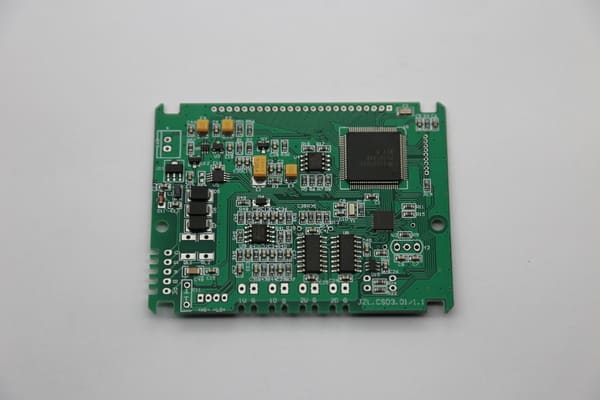
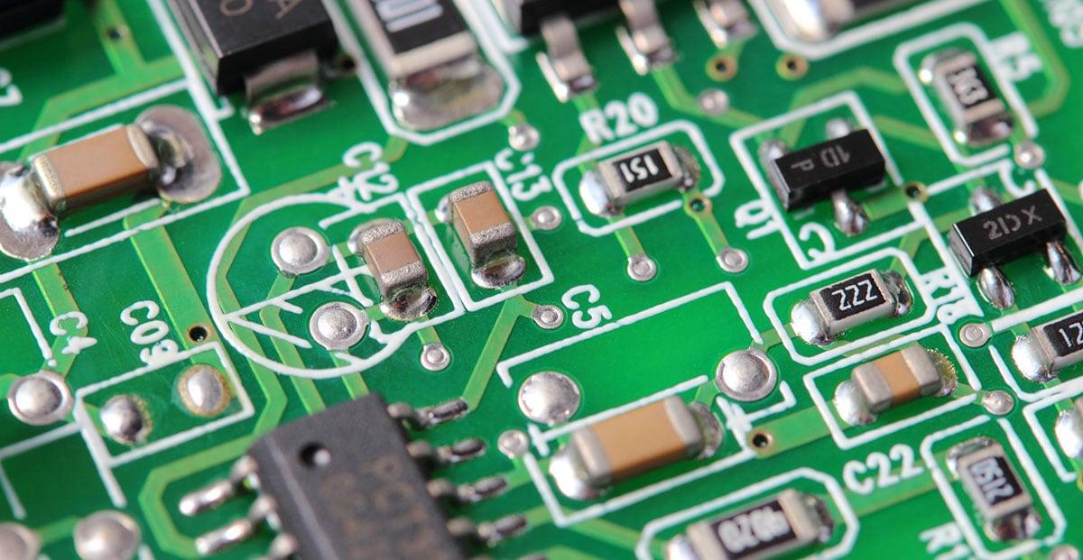
The silkscreen layer in PCB design is a printed overlay of text, symbols, and graphics applied directly to the surface of the board. It sits on top of the solder mask and is usually visible as white or yellow ink against the green, red, or black background of the board. Its primary job is to communicate information—telling assemblers where each component goes, which direction it faces, and what value or reference designator it carries.
Common elements found on a PCB silkscreen include component reference designators (R1, C3, U2), pin-one indicators for integrated circuits, polarity markings for diodes and electrolytic capacitors, connector labels, test point identifiers, board revision numbers, manufacturer logos, and regulatory symbols such as CE or RoHS marks. Together these elements transform a bare board into a self-documenting artifact that guides every hand that touches it.

Why the Silkscreen Layer Matters
Skipping or skimping on the silkscreen layer creates downstream problems that are far more expensive than the ink itself. Here is why every well-designed board should include a thorough silkscreen:
Assembly accuracy. Pick-and-place operators and manual soldering technicians rely on reference designators and polarity indicators to position components correctly the first time. A clear silkscreen reduces rework and scrap rates.
Troubleshooting and repair. Field technicians armed with a schematic and a board with readable labels can isolate faults quickly. Boards without silkscreen require constant cross-referencing with layout files, slowing diagnosis and increasing error risk.
Quality and compliance. Regulatory bodies often require identifiable marks such as serial numbers, UL listings, or country-of-origin text. The silkscreen is the standard location for these legally required elements.
Brand identity. Company logos and product names printed on the silkscreen reinforce professional presentation, which matters when a board is visible inside consumer electronics or industrial enclosures.
Silkscreen Application Methods
PCB manufacturers use several techniques to apply the silkscreen layer. Each method has its own trade-offs in resolution, cost, and turnaround time.
Liquid Photo Imaging (LPI)
Liquid photo imaging is the industry's most precise silkscreen method. A photosensitive epoxy ink is flooded across the board surface, then exposed to ultraviolet light through a film negative bearing the legend artwork. UV exposure cures the ink in exposed areas while the unexposed portions are washed away during development. LPI yields sharp, fine-line legends with excellent adhesion and is the preferred choice for high-density designs where component spacing is tight and text must remain legible at small font sizes.
Direct Legend Printing (DLP)
Direct legend printing uses an inkjet-style print head to deposit acrylic ink directly onto the board surface according to a digital file. Because no film or screen is required, DLP integrates easily into automated workflows and supports last-minute design changes without tooling costs. Resolution is generally lower than LPI, making DLP better suited for boards with modest spacing requirements, though continued improvements in inkjet head technology are steadily closing that gap.
Epoxy Ink Screen Printing
The original and still widely used approach, epoxy screen printing pushes ink through a fine mesh stencil stretched over a frame. It is cost-effective at high volumes and produces durable results, but its minimum line width is broader than LPI, and it is not ideal for boards where features are densely packed. For straightforward, mid-complexity designs produced in large batches, screen printing remains an economical workhorse.
Silkscreen Design Rules to Follow
Good silkscreen design is more than placing text wherever space permits. Following established design rules ensures the legend survives fabrication and remains readable:
Minimum text height. Keep character height at or above 1.0 mm (approximately 50 mil) and line width at or above 0.15 mm to ensure legibility after printing.
Keep ink off pads. Silkscreen ink printed over exposed copper pads interferes with soldering. Most EDA tools provide a design rule check that flags silkscreen-to-pad clearance violations; the typical minimum clearance is 0.1 mm.
Consistent orientation. Aligning text in a single direction—or at most two perpendicular directions—significantly reduces the chance of misreading a label during hand assembly.
Avoid silkscreen over vias. Ink can wick into open vias during application, causing registration errors and potentially creating contamination in through-holes.
Prioritize critical markers. If space is extremely tight, prioritize polarity markers and pin-one indicators over reference designators. A missing 'R12' label is inconvenient; a missing polarity mark can destroy a component.
Silkscreen Missing — What Happens and What to Do
A silkscreen missing scenario arises in several ways: the design file was submitted without a populated silkscreen layer, the layer was inadvertently left empty in the Gerber export, or the manufacturer omitted it to reduce cost. Regardless of the cause, the consequences ripple through production and support:
Assembly lines slow down as technicians must consult layout files for every component placement.
Polarity-sensitive components such as electrolytic capacitors and diodes face a higher risk of being installed backwards, leading to board failures or even component damage.
Field repair becomes significantly harder, especially for third-party service centers that may not have access to original design files.
Compliance audits may flag the board if mandatory regulatory markings are absent.
If you discover the silkscreen is missing before fabrication, update the Gerber files and resubmit. Most PCB fabricators, including online services, allow file resubmission at no extra charge before production begins. If the boards have already been fabricated without silkscreen and volumes are low, consider adding hand-written labels or using laser etching as a workaround. For future orders, double-check your Gerber export settings to confirm the silkscreen layer (typically named F.Silkscreen, GTO, or Top Overlay depending on your EDA tool) is included and populated.
Choosing the Right Silkscreen Color
White is the default silkscreen color and offers the highest contrast against the most common solder mask colors—green, red, blue, and black. Yellow is sometimes used on white solder mask boards. Black silkscreen works well on white or natural-finish boards. While color selection is partly aesthetic, contrast is the non-negotiable practical consideration: low-contrast silkscreen becomes difficult to read under production lighting and nearly impossible to photograph for automated optical inspection (AOI) systems calibrated for standard contrast ratios.
Working with a PCB Manufacturer on Silkscreen Specifications
When ordering boards, communicate your silkscreen requirements clearly in the fabrication notes or order form. Specify the color, the application method if you have a preference, and any minimum line-width or font-height constraints your design relies on. Reputable fabricators will run a design-for-manufacturability (DFM) check and flag potential issues—such as text that is too small for their process or silkscreen elements that overlap pad openings—before cutting the panels.
For projects ranging from prototypes to production runs, PCBgogo is a full-service fabricator that supports white and yellow silkscreen across LPI and direct-print processes. Uploading your Gerber files through their instant quote system lets you confirm silkscreen options and pricing in minutes, which is particularly useful when evaluating cost trade-offs between application methods for a given board complexity.
Silkscreen vs. Solder Mask: Understanding the Difference
Designers new to PCB fabrication sometimes confuse the silkscreen layer with the solder mask. They are distinct layers with different purposes. The solder mask is the colored coating—usually green—that covers the copper traces and base laminate, protecting them from oxidation and preventing solder bridges during assembly. The silkscreen is the ink layer printed on top of the solder mask, carrying only informational markings. One protects copper; the other communicates information. Both are essential, and both should be specified correctly in every Gerber export.
Final Thoughts
The printed circuit board silkscreen is one of those design elements that goes unnoticed when done well and causes real pain when neglected. A properly executed silkscreen layer reduces assembly errors, accelerates troubleshooting, satisfies regulatory requirements, and projects professionalism. Whether you are designing a one-off prototype or preparing for mass production, investing the time to populate, verify, and correctly export your silkscreen layer pays dividends at every stage downstream. Review your design rules, confirm your Gerber export, and partner with a manufacturer who reviews silkscreen specifications as part of their standard DFM process—your assembly team will thank you.





