
 日本語
日本語
 한국어
한국어

Fiducial Marks in PCB Design: What They Are, Why They Matter, and How to Design Them Right
Modern electronics keep shrinking while the number of components on a board keeps growing. Pick-and-place machines now place parts with pitches measured in fractions of a millimeter, and they cannot do that reliably by guessing where a board sits on the conveyor. They need a fixed, unmistakable reference point etched directly into the copper — a fiducial mark. This guide explains what fiducial marks are, the different types used in PCB assembly, why they improve manufacturing outcomes, and the practical design rules that keep them working the way they should.
What Is a Fiducial Mark?
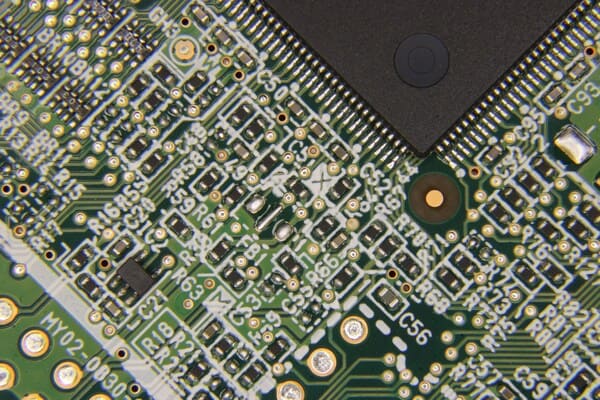
A fiducial mark (sometimes called an optical alignment mark or target point) is a small, precisely shaped area of exposed copper — most commonly a solid filled circle — placed on a PCB specifically so that automated equipment can locate it with a vision camera. Unlike drilled holes, mounting holes, or silkscreen dots, a fiducial mark is etched in the same process step as the copper pads and traces around it, so its position relative to every component footprint on the board is known with very high accuracy.
During assembly, machine-vision systems on stencil printers, pick-and-place machines, and solder paste inspection (SPI) equipment scan for these marks. Once the software finds them, it calculates the board's exact X/Y position and rotation angle, and adjusts every subsequent placement coordinate to match. In effect, fiducial marks act as a coordinate system printed directly onto the product itself.
Why Fiducial Marks Matter
Placement accuracy
Fine-pitch packages such as BGAs, QFNs, and 0201 passives leave almost no room for error. Fiducial marks let the placement machine correct for small manufacturing variations — panel shift, board rotation, or minor warping — before a single component touches the board.
Faster, more repeatable production
Because the vision system finds its bearings automatically, operators do not need to manually align each panel. This shortens setup time between jobs and keeps placement accuracy consistent from the first board of a run to the last.
Better inspection and quality control
Automated optical inspection (AOI) and solder paste inspection systems also use fiducial marks as a fixed reference frame, which makes it easier to catch shifted components, insufficient solder paste, or other defects early in the process rather than after reflow.
A more reliable reference than holes or silkscreen
Tooling holes and silkscreen markings are added in separate manufacturing steps and can vary in size, position, or visibility — and they may end up partially covered by solder mask. A properly designed fiducial mark is standardized in shape, exposed copper, and free of coating, so it gives the vision system a consistent target every time.
Types of Fiducial Marks
Not every fiducial mark serves the same purpose. Depending on where they sit on the board or panel, they fall into a few recognized categories.
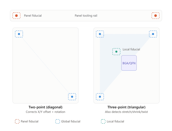
Panel fiducials — Placed on the assembly panel's tooling rails, these align the entire panel with the stencil printer and placement equipment before any individual board is processed.
Global fiducials — Usually positioned in two or three corners of an individual PCB, on a diagonal or triangular pattern, these establish the position and orientation of the whole board.
Local fiducials — Smaller marks placed close to individual fine-pitch components (footprints with less than roughly 0.5 mm pitch), used to fine-tune placement accuracy for that specific part rather than the whole board.
Two global fiducial marks are enough to correct simple X/Y offset and rotation. A third mark, arranged so the three are not in a straight line, allows the vision system to also detect and compensate for non-linear distortion — stretch, shrink, or twist — that can occur in larger panels or during thermal cycling. For that reason, a three-point global layout is generally considered the better practice for boards with fine-pitch parts, double-sided assembly, or larger panel sizes.
Fiducial Mark Design Guidelines
The specific numbers vary a little between fabrication houses and assembly lines, but the following table summarizes the values most commonly recommended in the industry.
| Design Element | Recommended Value | Basis / Standard | Why It Matters |
|---|---|---|---|
| Shape | Solid filled circle | IPC / SMEMA | Same silhouette at any rotation angle |
| Diameter | 1.0 mm – 3.0 mm | IPC / SMEMA | Balances contrast area vs. board space |
| Size consistency | Variation ≤ 25 μm on one board | IPC | Lets vision software reuse one threshold |
| Clearance (keep-out) diameter | 2–3× the fiducial diameter | Common practice | Keeps silkscreen/traces from confusing the camera |
| Surface | Bare copper, no mask/coating | IPC / SMEMA | Maximizes optical contrast |
| Flatness | ≤ 15 μm | High-precision SPI practice | Stable Z-axis reference for 3D SPI |
| Distance to board edge | ≥ 5 mm (min. ~3.85 mm) | SMEMA transport clearance | Avoids clamps, rails and conveyor contact |
A few additional points worth keeping in mind when placing marks in a layout:
1. Double-sided boards — If components are mounted on both sides of the board, add a full set of fiducial marks to each side. Without marks on the second side, the equipment has nothing to align to when the board is flipped.
2. Don't over-add marks — Avoid a fourth global mark in the unused corner unless your assembly house specifically asks for it — an extra mark can add ambiguity to the vision system's reference model instead of improving it.
3. Stay clear of scoring lines — Keep marks away from panel V-cut or tab-route lines. The mechanical stress of depaneling can crack nearby features, so a buffer of several millimeters is good practice, especially on thinner boards.
4. Flex PCB considerations — On flexible and rigid-flex circuits, anchor each fiducial to a solid copper area rather than letting it sit alone on the polyimide film, since flex material can stretch or shrink slightly during processing.
5. Choose a stable surface finish — Bare copper with ENIG or immersion tin finishes tends to give the most even, predictable reflectivity for vision systems. Uneven finishes such as HASL can create surface irregularities that make detection less reliable.
Common Mistakes to Avoid
Inconsistent diameters: Marks on the same board differ by more than ~25 μm, forcing the vision system to second-guess its threshold.
Low contrast: Using a solder-masked or plated pad instead of bare copper makes the mark hard to distinguish from the background.
Cluttered keep-out zone: Silkscreen text, traces, or vias inside the clearance ring interfere with centroid detection.
Only two global marks on a large or double-sided board: Two points fix translation and rotation but cannot correct stretch, shrink, or twist.
A redundant fourth global mark: Extra marks can confuse the geometric reference model instead of helping it.
Using tooling holes or silkscreen dots as marks: These are not etched with the same precision as copper features and register less accurately.
Placing marks too close to the board edge or V-cut lines: Clamps, rails, and depanelization stress can damage or obscure marks placed less than ~5 mm from an edge.
No copper anchoring on flex circuits: Without a solid copper tie-in, a fiducial can drift as flexible material stretches or shrinks.
Conclusion
Fiducial marks look like a minor detail on a finished PCB, but they are what allow automated assembly lines to place components with sub-millimeter accuracy, run efficiently, and catch defects before they become field failures. Getting the basics right — consistent size, bare copper, adequate clearance, sensible placement, and enough marks to correct for distortion — pays off directly in higher first-pass yield and fewer placement errors. Whether you are laying out your first prototype or refining a design for high-volume production, treating fiducial marks as a core part of the PCB layout, not an afterthought, is one of the simplest ways to improve assembly outcomes.





