日本語
 한국어

Solder Paste Inspection: A Practical Guide to Better PCB Assembly
Solder paste inspection checks each printed paste deposit before components are placed. In a well-controlled SMT line, it catches missing, excessive, or shifted paste while the board can still be cleaned and reprinted. The useful output is not just a pass or fail result: deposit measurements show whether the stencil printing process is drifting.
A board can pass bare-board electrical test and still fail after assembly because one fine-pitch pad received too little paste. Finding that fault after reflow means rework; finding it immediately after printing means fixing the print. This guide explains what to measure, how to act on failures, and where SPI fits with later checks.
Key Takeaways
KEY TAKEAWAYS Check paste before placement; judge deposits against the board's pad and stencil design; investigate repeated patterns rather than treating every alarm as an isolated board. SPI is most valuable when its data leads to a specific printer, stencil, paste, or support adjustment.
What Is Solder Paste Inspection
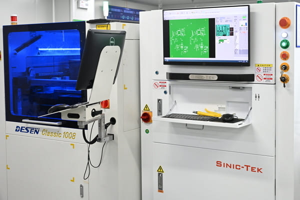
Solder paste inspection (SPI) examines paste deposits on PCB pads after stencil printing and before component placement. A 2D system checks appearance and coverage; a 3D system also measures deposit height and volume. Inspection limits should follow the actual aperture design and assembly risk, because a single universal volume target is unsuitable for every pad.
Why Solder Paste Inspection Matters
Poor paste printing can become an open joint, bridge, or uneven solder joint after reflow. At the SPI stage, there are no components to remove, so a board with a confirmed print defect can usually be cleaned and reprinted under the assembler's approved procedure. That makes SPI an early process-control step, especially for fine-pitch ICs and small passives where adjacent deposits have little separation.
A failed deposit does not prove the finished joint would fail. It signals a print condition that deserves review before more value is added to the PCB. This distinction matters when setting limits: overly tight thresholds create false calls, while loose ones allow unstable printing to continue.
Key Parameters in Solder Paste Inspection
The measurements below answer different questions. Review them together rather than accepting a deposit because one number looks normal.
| Parameter | What it reveals | Useful response to a repeated failure |
|---|---|---|
| Volume | Paste quantity per deposit | Check aperture release, stencil cleanliness, paste condition, and squeegee settings. |
| Height and area | Deposit profile and footprint | Check stencil contact, board support, and whether paste is spreading. |
| X/Y offset | Position relative to the pad | Check board registration, fiducials, and stencil alignment. |
| Shape or bridging | Smears, tails, or connected deposits | Inspect the stencil underside and local pad spacing before restarting. |
Solder Paste Inspection Steps
A useful SPI routine ties each result to a decision on the line:
Prepare the program from PCB and stencil data. Confirm board orientation, fiducials, pad mapping, and the expected deposits before production.
Inspect the first printed board. Review critical pads manually and set product-specific limits using approved process criteria, not an arbitrary percentage copied from another design.
Run inline inspection after printing. Segregate confirmed failures before placement; clean and reprint only when the work instruction permits it.
Trend results across boards. A gradual volume drop or a repeating offset points to a process cause. Correct that cause, then verify the next prints before releasing the line.
Typical Defects Found by Solder Paste Inspection
Missing or low-volume paste may reflect a blocked aperture or poor paste release. Excess paste and smearing can connect neighboring pads; offset deposits suggest registration trouble. A print that is low across one board edge may instead indicate poor board support or uneven stencil contact. The pattern across pads and boards is often more useful than the single failed image.
Do not use SPI to declare solder joints good. Wetting, component movement, voids, and hidden joints are assessed after placement and reflow with the appropriate inspection or test method.
How 3D SPI Improves PCB Manufacturing
3D solder paste inspection adds measured height and volume to the 2D footprint. That helps distinguish a wide, thin smear from a deposit with the intended amount of paste, a difference that area alone can miss. The measurements also allow a process engineer to compare the same pad over successive boards and identify drift before failures multiply.
For example, if several pads fed by one stencil region show falling volume, inspect aperture clogging and stencil wiping before changing placement settings. If many deposits shift in the same direction, check registration first. Automatic printer feedback can help where equipment is integrated, but the correction still needs verification against a new print.
The Role of SPI Across the SMT Line
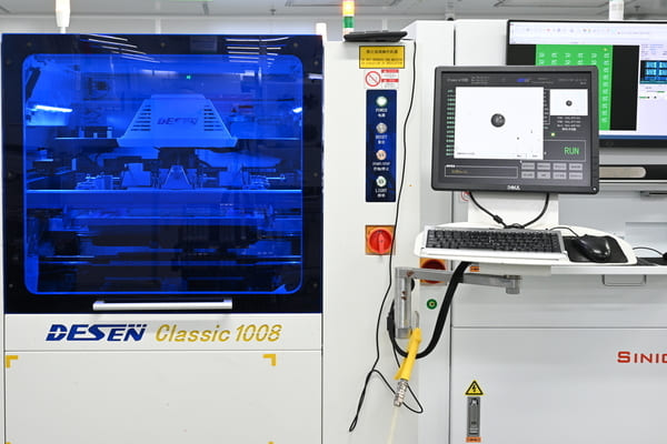
The practical sequence is stencil print → SPI → component placement → reflow → post-reflow inspection and test. SPI controls the print; AOI checks visible placement and soldering outcomes; X-ray can examine joints hidden under packages such as BGAs. These checks answer different questions, so a passing SPI result never replaces downstream inspection.
For a customer reviewing an assembly quote, ask how the supplier handles SPI failures and whether print trends trigger corrective action. Also ask which post-reflow checks apply to hidden-pad parts and how first-article results are approved. Those answers reveal more about process control than an equipment list alone.
PCBgogo for Consistent SMT Assembly Quality
When paste printing is a risk, the assembly partner should inspect it before placement and keep later checks in the workflow. PCBgogo lists full-coverage SPI for insufficient, excessive, or misaligned paste, along with AOI and X-ray inspection for later assembly stages. Share your PCB files, stencil requirements, component list, and any critical joints when requesting a PCB assembly quote so the inspection plan can match the design.
PCBgogo - Reliable, High-Quality PCB Manufacturing
PCBgogo is a one-stop PCB and PCBA manufacturing factory, helping you save time and costs while ensuring consistent, reliable quality.
Get a Free Quote >
FAQ
Can SPI detect a bad solder joint?
No. SPI examines printed paste before solder joints exist. Post-reflow AOI, X-ray where appropriate, and electrical or functional tests address different failure modes.
Is 3D SPI always necessary?
Not every assembly needs the same inspection depth. 3D measurement is especially useful when deposit volume or height matters, such as fine-pitch pads or small passives, but the choice should reflect the design and process risk.
What should happen after repeated low-volume alarms?
Stop releasing affected boards and check whether the pattern is local or board-wide. Inspect the stencil aperture, wipe cycle, paste condition, printer setup, and board support; then confirm the correction on fresh prints.