日本語
 한국어

Fine Pitch Assembly Guide for Reliable PCB Production
KEY TAKEAWAYS Fine pitch assembly succeeds when package geometry, PCB layout, solder-paste printing, placement, reflow, and inspection are treated as one process. For each fine pitch component, confirm the footprint, escape routing, stencil, fiducials, and test access before release.
Fine pitch assembly leaves little room for variation. Errors in the land pattern, stencil, board flatness, or placement data can cause bridging, opens, insufficient solder, and costly rework. The goal is a repeatable process from design release through inspection.
What Is a Fine Pitch Component
A fine pitch component is a surface-mount package with closely spaced leads or pads, such as QFP, QFN, BGA, LGA, and small passives. Risk rises as pitch, pad area, solder volume, and inspection access shrink, so pitch alone cannot determine fine pitch assembly feasibility.
A 0.5 mm QFP has exposed leads that AOI can inspect; a 0.5 mm BGA hides its joints and may need via-in-pad or microvia routing. Before layout, record pitch, pad style, body size, moisture sensitivity, and reflow requirements.
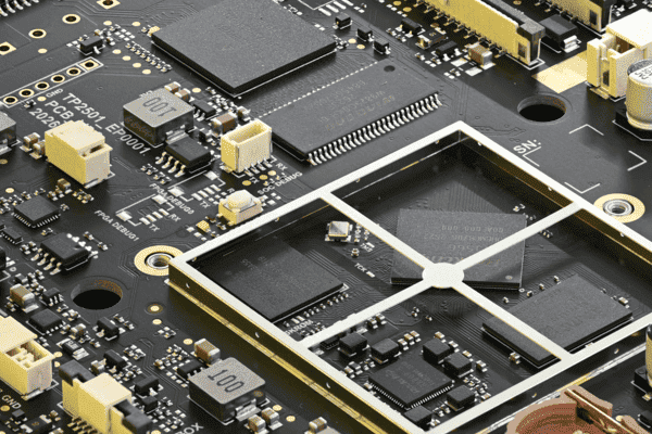
Fine Pitch PCB Design and Layout
A manufacturable fine pitch PCB assembly aligns the package footprint, stackup, routing, assembly tooling, and inspection plan before traces are committed. The following decisions have the largest effect on yield.
Component selection. Choose packages with complete drawings, land patterns, thermal guidance, and stable supply. Verify pin one and any baking or rework requirements.
Board size and stackup. Limit warpage and confirm trace, spacing, drill, microvia, and BGA escape limits before placement is frozen.
Component placement. Keep devices away from edges, tabs, tall parts, and flexing areas. Give cameras clear fiducial access and orient similar ICs consistently.
Pads and vias. Use the supplier footprint and a consistent solder-mask strategy. Open vias can wick solder; specify filled and planarized vias when via-in-pad is required.
Decoupling capacitors. Place them close to power pins with a short plane return. Avoid long neck-down traces or shared vias while retaining assembly clearance.
Fiducials, tooling holes, and test points. Use global and, where needed, local fiducials with solder-mask clearance. Match tooling holes to panel handling and keep test points accessible.
Use this release check to connect design choices with production controls:
| Design item | Release check | Defect reduced |
|---|---|---|
| Land pattern | Supplier drawing and polarity match the CAD library | Bridging and opens |
| Stencil | Apertures reviewed by package type and paste-release risk | Excess or insufficient solder |
| Placement data | Centroids, rotations, side, and reference designators verified | Misalignment and wrong orientation |
| Inspection | AOI, X-ray, and test coverage assigned by joint visibility | Escaped defects |
How to Achieve High Quality Fine Pitch PCB Assembly
High-quality fine pitch assembly depends on controlling variation at each process gate, not relying on final inspection to sort defects.
Review the data. Align Gerbers, notes, BOM, centroid file, polarity, package names, substitutions, and revisions. Resolve footprint or rotation conflicts before programming.
Control paste printing. Match stencil thickness and apertures to small deposits and thermal pads. SPI should catch paste volume and offset errors before placement.
Stabilize placement and reflow. Support the PCB, verify feeder setup and first article, then profile the actual board and paste. Change one process variable at a time during troubleshooting.
Inspect by risk. Use AOI for visible features, X-ray for hidden BGA and QFN joints, and electrical or functional tests for circuit behavior.
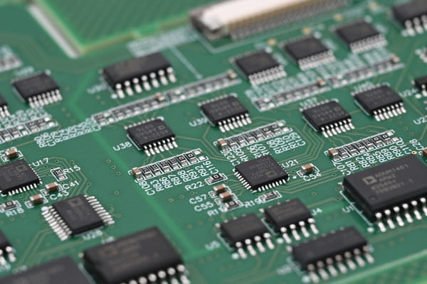
PCBgogo Fine Pitch PCB Assembly Capabilities
A fine pitch assembly partner should connect design review, fabrication, sourcing, assembly, inspection, and test under one controlled workflow. PCBgogo publishes the following capabilities for fine pitch assembly projects that include a fine pitch component:
Fine-pitch support: assembly of components down to 0.25 mm pitch, including QFN and BGA package types.
Small-package placement: 01005 passives and published mounting accuracy of ±0.035 mm, with a stated high-precision condition of ±0.025 mm at Cpk ≥1.0 (3 sigma). Feasibility still depends on package and board design.
Hidden-joint inspection: X-ray inspection for high-precision packages with concealed pads, supported by SPI, AOI, visual inspection, and first-article checks.
One-stop delivery: PCB fabrication, sourcing, stencil preparation, SMT and through-hole assembly, and testing in one workflow.
Quality control: incoming and in-process inspection, SPI, AOI, X-ray, and customer-defined functional testing support fine pitch assembly quality.
PCBgogo - Reliable, High-Quality PCB Manufacturing
PCBgogo is a one-stop PCB and PCBA manufacturing factory, helping you save time and costs while ensuring consistent, reliable quality.
Get a Free Quote >
Summary
Reliable fine pitch assembly starts with package-aware PCB design and continues through controlled printing, placement, reflow, inspection, and testing. With more than 10 years of fine pitch PCB assembly and manufacturing experience, PCBgogo is a reliable one-stop PCB manufacturing partner for prototypes and production builds.
Frequently Asked Questions
What files are needed for a fine pitch assembly quote
Provide Gerber or ODB++ data, fabrication notes, BOM, centroid file, assembly drawings, and test requirements. Keep all files on one revision and flag any fine pitch component needing special handling.
Does every fine pitch component require X-ray inspection
No. AOI can inspect exposed QFP leads, but hidden BGA, LGA, and QFN joints normally need X-ray. Electrical or functional testing is still required when imaging cannot prove circuit performance.
Should vias be placed inside fine-pitch pads
Only when the routing requires via-in-pad and the fabricator can fill and planarize the vias. Open vias can pull solder away from the joint, so the via structure and finished pad must be agreed before releasing the fine pitch assembly design.
How can solder bridging be reduced
Verify land pattern and solder mask, optimize stencil apertures, control paste with SPI, and support the PCB during printing. In fine pitch assembly, stable paste deposition is often the first process to investigate.