



 日本語
日本語
 한국어
한국어

Laser Direct Imaging: How LDI Transforms PCB Manufacturing
As electronics grow smaller and more complex, the methods used to manufacture printed circuit boards must keep pace. Laser direct imaging PCB technology — commonly known as LDI — has emerged as one of the most significant advances in modern PCB fabrication. By replacing traditional photomask-based exposure with a digitally controlled laser, LDI delivers a level of accuracy and repeatability that older processes simply cannot match. This article explores how laser direct imaging works, why it outperforms conventional photolithography, and which applications benefit most from adopting it.
What Is Laser Direct Imaging?
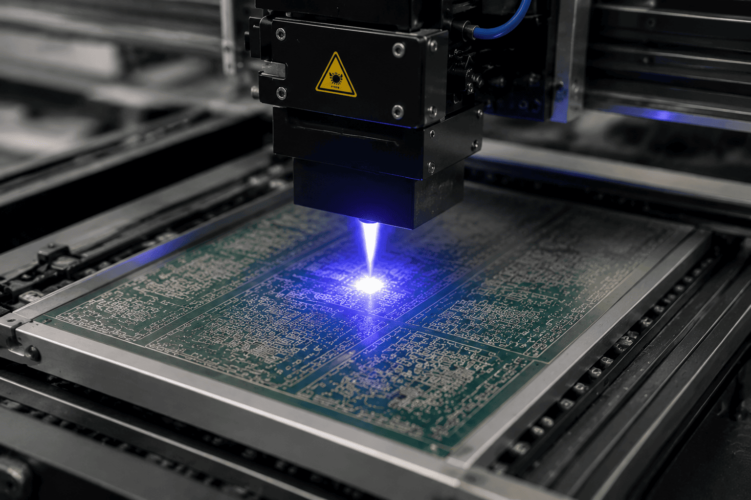
Laser direct imaging is a PCB exposure process in which an ultraviolet (UV) laser beam writes circuit patterns directly onto a photosensitive resist coating — with no physical mask or film artwork involved. The laser is guided entirely by digital design data, so the pattern transferred to the board is an exact reproduction of the CAD file. Once exposed, the resist is developed and the underlying copper is etched or plated to form the final circuit traces.
The key difference from traditional methods is the elimination of the photomask. Conventional photolithography requires producing a physical mask for every new design, a step that introduces cost, lead time, and the risk of dimensional error. LDI skips that step entirely, making it faster to prototype and more consistent across production runs.
How the LDI Process Works
Understanding the LDI workflow helps clarify why it produces superior results. The process follows these stages:
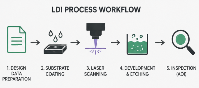
Design data preparation: The PCB layout file is loaded directly into the LDI system's software. No film generation or mask production is required.
Substrate coating: The bare PCB panel is coated with a photosensitive dry-film or liquid resist and loaded into the machine.
Laser scanning: A high-speed UV laser scans across the resist surface, exposing only the areas that correspond to the circuit pattern. Modern LDI systems use multiple laser channels in parallel to maintain throughput.
Development and etching: The exposed board moves through conventional chemical development and etching or electroplating, as with any photolithographic process.
Inspection: Automated optical inspection (AOI) verifies the finished pattern against the original CAD data.
Because the laser position is recalculated in real time, the system can also compensate for panel expansion or contraction caused by temperature and humidity — a critical advantage when working with thin or flexible substrates.
LDI vs. Traditional Photolithography
Traditional photolithography uses a UV light source to expose the resist through a physical photomask held against the board surface. While this method works adequately for standard-density designs, it has several structural limitations:
Mask degradation: Physical masks wear over time and must be replaced, adding recurring cost and the risk of subtle dimensional drift.
Alignment errors: Positioning a mask precisely over a panel — layer after layer — introduces cumulative registration error, especially on multilayer boards.
Resolution limits: Light scatters at the edges of mask features, limiting minimum trace widths to around 75–100 micrometers reliably.
Prototype lead time: Every design change requires a new mask, adding days to the development cycle.
Laser direct imaging addresses each of these issues directly. The digital process has no mask to degrade, registration is handled by software with micron-level corrections, minimum trace/space widths drop to 50 micrometers or below, and design changes are implemented instantly by updating the CAD file. The result is a process that is simultaneously more precise, more flexible, and more cost-effective at scale.
Applications That Benefit Most from LDI
Laser direct imaging is not limited to any single product category. Its combination of precision and speed makes it valuable across a wide range of demanding applications:
High-density interconnect (HDI) boards: Smartphones, tablets, and wearables rely on HDI designs with fine-pitch BGA pads and microvias. LDI handles these geometries reliably and consistently.
Flexible and rigid-flex PCBs: Flex substrates shift dimensionally during processing. LDI's real-time compensation prevents pattern misalignment on these difficult materials.
5G and RF circuits: High-frequency designs require extremely tight impedance control, which depends on precise trace geometry. LDI's sub-50-micrometer accuracy is essential here.
Medical and aerospace electronics: Industries where board failure is not an option demand the repeatability and traceability that digital LDI processes provide.
Rapid prototyping: Engineering teams that need to iterate quickly benefit from LDI's maskless design, since new revisions can be run without tooling delays.
Key Advantages of Laser Direct Imaging PCB Technology
Summarizing the practical benefits, LDI offers manufacturers and designers:
Higher resolution: Line and space widths below 50 micrometers are achievable, enabling next-generation miniaturized designs.
Improved layer-to-layer registration: Software-driven alignment compensates for real-world panel variation, reducing defects in multilayer boards.
Faster design iteration: No mask production means design changes can be in production within hours rather than days.
Lower defect rates: Removing the physical mask eliminates an entire class of defects related to mask contamination, scratches, and dimensional shift.
Scalability: LDI scales well from prototype quantities through high-volume production without process re-qualification.
Choosing the Right PCB Manufacturing Partner for LDI Projects
Not every PCB manufacturer has invested in laser direct imaging equipment. When sourcing boards that require fine-pitch traces, tight registration tolerances, or flexible substrates, verifying that your manufacturer operates LDI systems is an important step in the qualification process.
For engineers and procurement teams looking to work with an experienced manufacturer, PCBgogo offers PCB fabrication services with support for advanced process requirements including HDI and fine-line designs. You can upload your Gerber files and request an instant quote directly from their platform, making it straightforward to verify manufacturability and pricing before committing to a production run.
Conclusion
Laser direct imaging represents a genuine technological step forward for PCB manufacturing. By moving pattern transfer from a physical, analog process to a digital, software-driven one, LDI achieves resolution and repeatability that traditional photolithography cannot replicate. For designers working on HDI boards, flexible circuits, RF applications, or any project where trace geometry directly affects performance, specifying a manufacturer with LDI capability is not simply a preference — it is a quality requirement.
As electronic products continue to shrink while their complexity increases, laser direct imaging PCB technology will only become more central to the fabrication process. Engineers who understand what LDI offers — and who choose manufacturing partners equipped to deliver it — will be better positioned to bring reliable, high-performance products to market.





