
What is PCB Etching? A Precision Process Like 'Carving Art'
In the manufacturing of PCBs, there is one process that most embodies a sense of transformation, turning something basic into something magical. It’s not as tangible as components, but it shapes the very soul of the circuit board: the delicate and complex circuit traces. This process is called etching. It’s less like industrial production and more like a piece of intricate "carving art," sculpting the pathways for electronic information to flow on a copper-clad board.
The Essence of Etching: Creating Through Subtraction
PCB etching is a "subtractive manufacturing" process. The core idea is to first protect the parts of the copper we need, and then, through a chemical reaction, dissolve away the unwanted copper, leaving behind the precisely designed circuit lines. The process is much like a sculptor who first sketches a desired pattern on a flat stone with a wax pencil, then uses a chisel to remove the excess material, finally revealing a beautiful work of art.
This seemingly simple process is full of challenges and artistry in actual production.
The "Carving" Process: A Step-by-Step Look
Etching typically follows a strict, multi-step process to ensure every detail is perfect.
Preparing the "Canvas" and Creating the "Stencil": First, we start with a base board covered with a layer of copper foil, which is our "canvas." We then cover the copper surface with a special photosensitive dry film or photoresist. This film is then exposed to UV light through a negative film of the circuit pattern. The exposed areas of the photosensitive material will undergo a chemical reaction and harden.
Developing: Outlining the Circuit After exposure, the board is rinsed with a chemical developer. The unexposed parts of the photosensitive material (the areas where we don't want copper lines) are dissolved and washed away. The hardened, exposed parts (the areas where we do want copper lines) remain, firmly attached to the copper foil. At this point, the copper on the circuit board has a clear outline of the circuit pattern, just as a sculptor would have sketched the lines of their design.
Etching: Removing the Excess Copper: This is the most crucial step. The circuit board is submerged in or sprayed with an etching solution (such as Ferric Chloride or Ammoniacal etchant). The etchant only reacts with and dissolves the bare, exposed copper, leaving the copper protected by the photoresist untouched. This process is like using a special "potion" to "carve," melting away only the unwanted copper.
The Final "Reveal": Stripping the Protective Layer: Once the etching is complete, all the excess copper foil has been removed. The final step is to use a special stripping solution to clean off the remaining protective photoresist layer. At last, the intricate and complete copper circuit lines are revealed on the board.
The Challenge of Precision and Environmental Responsibility
In today's electronics industry, the demand for PCB trace precision is constantly increasing. For example, circuit boards used in 5G communication and AI chips may have trace widths of only a few micrometers, much finer than a human hair. This requires the etching process to be incredibly precise, as any over-etching or under-etching could lead to short circuits or open circuits, rendering the entire board useless.
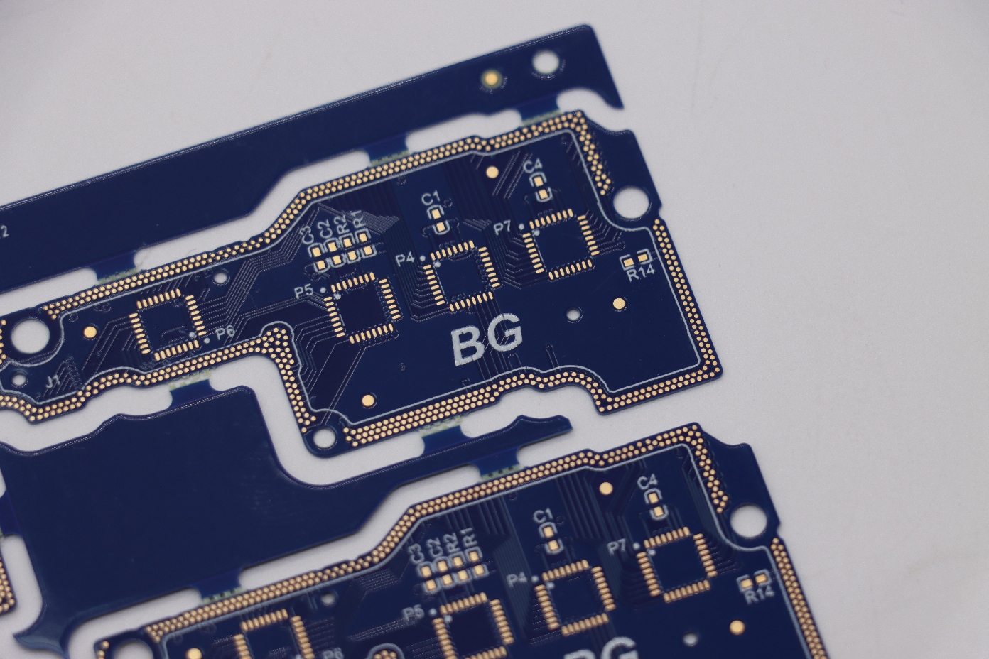
At PCBgogo, we deeply understand the precision and challenges of etching. We see it as a blend of technology and art, and the birth of every board is a testament to our craftsmanship in this "carving art." We continuously introduce the most advanced etching equipment and strictly control every process parameter to ensure that every single trace is as precise as the original design. Simultaneously, we place a high value on environmental protection, having established a comprehensive waste treatment system to ensure that while we pursue ultimate precision, we also act responsibly toward the environment. We believe that only by striving for excellence in every detail can we provide customers with truly reliable and high-performance PCB products.

