PCB Vias: Types, Design, Covering
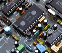
Due to the miniaturization of electronic products and the increasing complexity of PCB design, multi-layer boards are widely used, of them vias are one of the important structures that establish connections between isolated copper layers.
Types of vias
Vias either serve as the electrical connection between layers or are used for fixing or positioning devices. There are three commonly seen vias: Through-hole, Blind via, and Buried via.
Through-hole
Through-hole is the most common type of hole which goes from one side of the circuit board to the other side. Through holes includes plated through holes (PTH) and non-plated through holes (NPTH). The way to distinguish them is to see if there is a layer of copper plating inside the hole wall. Vias are made by drilling. As the interior of the PCB is an insulating material, electroplating is applied to allow the electrons to move and conduct electricity.

Figure 1 NPTH versus PTH
The diameter of NPTH is usually larger than that of PTH because most NPTH is the mechanical hole necessary for securing the boards to work stable throughout the manufacturing process. Some might also be used as locking screws, and some to install the external connector. Some NPTH is also designed on the break-away of PCB to position the test fixture.
Plated through-holes can be used for internal interconnects or as mounting holes for leaded components. The diameter of these holes must be larger than the diameter of the weld leg of the component so that it can be inserted into the hole for assembly. Being easier to manufacture in technology and lower in cost, Through-holes are used on most printed circuit boards. However, some circuit layers do not need to connect with each other while a through-hole will take up extra space.
Blind via
Blind via is the connection between the outermost layer of the PCB and the adjacent inner layer with a plated hole that does not penetrate the entire board. The holes are visible from one side of the board, but not from the other side. This kind of via has a certain depth that usually does not exceed a certain ratio. Take a 6-layer board as an example, the plated holes connecting the first layer and the second layer, or the fifth layer and the sixth layer are blind vias.
Buried via
Buried via are located in the inner layer of the printed circuit board, which connects any inner circuit layer but does not conduct to the outer layer. It is invisible from the surface of the PCB. The manufacturing process of buried vias is much more complicated and expensive than the above two types of vias. Usually, such holes are used on HDI PCBs to increase the available space for other circuit layers.

Figure 2 Types of vias
Special design-Via in pad
With the miniaturization of electronic components and the prevalence of BGA packages, via in pad, placing the vias in the copper pad of the PCB becomes popular. The use of via-in-pad allows smaller and compact routing for fine components, which further reduces the PCB's overall size. However, if the solder melts and leaks into the via or the bottom layer through the via during the soldering process, it might lead to reliability defects such as insufficient solder in the solder joint, virtual soldering, and tombstone.
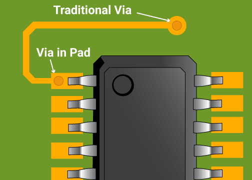
Figure 3 Via in pad
Via Covering-Tenting via
You might notice that some vias on a circuit board are covered with a solder mask over the annular rings. That’s because, during the manufacturing process, solder paste may remain on the vias. When the board flows through the reflow oven, the solder melts and is likely to flow from the via to the other side of the board, causing a short circuit problem. To avoid such quality problems, a tent-like shape is made over the hole to cover the via which not only ensures electrical performance but also reduces the possibility of shorts with other components. In some PCB manufacturers like PCBGOGO, tenting via is a default option. You can also choose other via covering such as plugged vias, that is to partially fill the insulation materials inside the via.
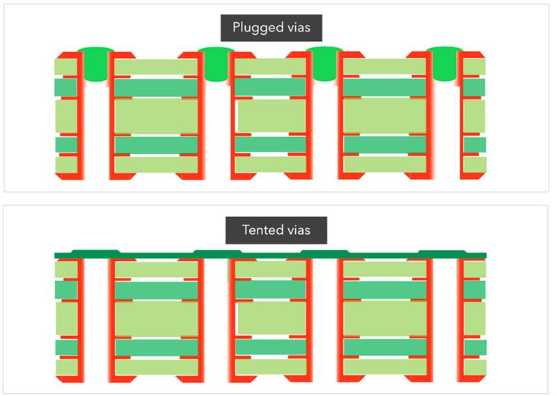
Figure 4 Plugged vias versus tenting vias
Conclusion
Drilling holes is critical in the PCB manufacturing process. The quality of vias directly affects whether the PCB can function normally. Nowadays, the increasingly complex and dense routing puts forward high requirements on PCB design and manufacturing techniques. In order to ensure the reliability of the final board, you should work with a reliable PCB manufacturer that can meet your design requirements. As a leading PCB manufacturer with vast industry experience, PCBGOGO can help you with the vias technology suitable for your projects.


