日本語
 한국어

Chips vs Semiconductors vs Integrated Circuits: A Practical PCB Guide
KEY TAKEAWAYS Chips vs Semiconductors vs Integrated Circuits describes three levels of electronics: semiconductors are materials or device classes, integrated circuits combine many functions on a die, and chips are dies or packaged devices. PCB footprints, power delivery, thermal paths, and assembly controls are selected for the package, not the silicon alone.
Key Takeaways
Semiconductor: a controllable material or device class, including silicon, silicon carbide, and gallium nitride.
Integrated circuit: many elements fabricated on one die for logic, memory, sensing, or control.
Chip: a practical umbrella term for a die or packaged semiconductor device; on a PCB BOM it usually means the packaged component.
PCB action: use the exact package drawing, land pattern, thermal data, and moisture sensitivity level.
Introduction
A sourcing team may call a MOSFET, microcontroller unit, and memory device "chips," but a PCB engineer must distinguish die, package, and function. This guide connects Chips vs Semiconductors vs Integrated Circuits to layout, assembly, and reliability decisions.
Chips
A chip is a semiconductor die containing a device or circuit, although the word often includes the package. Bare dies need die attach plus wire bonds or flip-chip interconnects; packaged chips connect through leads, pads, or solder balls. Record the full part number and package code because similar chips can have incompatible footprints.

Semiconductors
A semiconductor is a material whose conductivity can be controlled by doping, electric fields, light, or temperature. Material choice affects switching loss, voltage capability, operating temperature, cost, and the PCB's thermal and insulation strategy.
The table compares common semiconductor materials and the electronic roles they typically serve.
| Material | Useful Property | Typical Electronic Applications | PCB Implication |
|---|---|---|---|
| Silicon Si | Mature, economical | MCUs, memory, analog ICs, lower voltage power | Follow thermal-pad and decoupling guidance |
| Silicon carbide SiC | Wide bandgap, high temperature | High-voltage inverters, chargers, motor drives | Control creepage, switching loops, and heat |
| Gallium nitride GaN | Fast switching and low charge | Compact power conversion and RF | Minimize gate and power loop inductance; manage fast edge EMI |
| Gallium arsenide GaAs | High mobility and RF performance | RF front ends, microwave, optoelectronics | Use controlled impedance and low-loss materials |
Integrated Circuits
An integrated circuit is a network of active and passive elements fabricated on one die. CPUs, memory, op amps, and LED drivers are integrated circuits; a discrete diode or MOSFET is not. Place local decoupling close to power pins, isolate sensitive analog nodes from switching paths, and follow exposed-pad copper and via guidance.
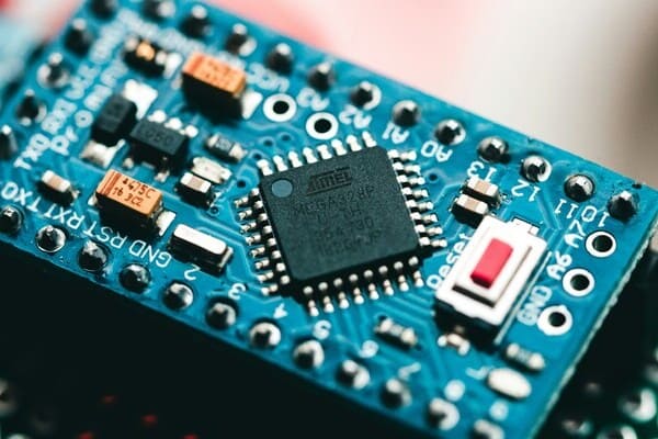
Chips, Semiconductors and Integrated Circuits at a Glance
This comparison separates material, function, and board-level form so teams can use each term precisely.
| Term | What It Identifies | Example | PCB Decision It Drives |
|---|---|---|---|
| Semiconductor | Material or device category | Silicon, SiC MOSFET | Voltage spacing, thermal design, switching layout |
| Integrated circuit | A complete circuit on one die | MCU, memory, LED driver | Power integrity, signal integrity, pin escape, firmware interface |
| Chip | Die or packaged device in common usage | QFN MCU or bare display driver die | Package, footprint, assembly process, inspection method |
How Chips, Semiconductors and Integrated Circuits Connect
The hierarchy is material, device structure, die, package, then PCB assembly. Fabrication forms devices and interconnects on semiconductor wafers; dicing creates chips; packaging exposes connections; assembly solders the package to PCB pads. Debug silicon behavior, package integrity, solder joints, and routing separately.
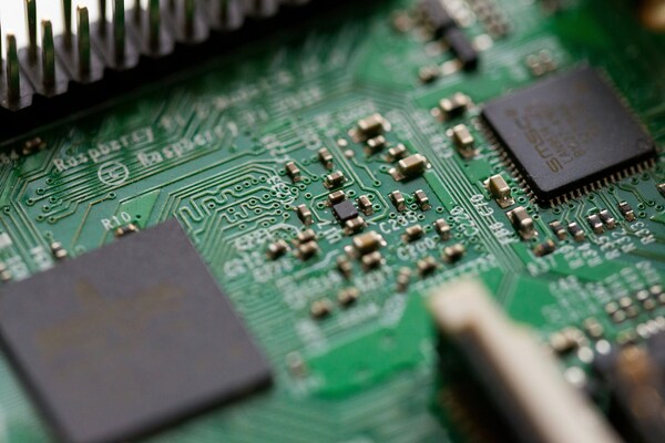
Semiconductor Manufacturing Process
Semiconductor manufacturing patterns and connects microscopic regions on a wafer before each chip is packaged and tested:
Prepare a high-purity wafer and form insulating and functional films.
Apply photoresist, expose a pattern, develop it, and etch selected regions.
Add dopants by implantation or diffusion to create device regions.
Deposit and pattern multiple metal layers that connect the transistors.
Probe the wafer, dice it into chips, attach each good die, connect it, encapsulate it, and complete final test.
PCB teams control package compatibility. Cross-check the BOM, datasheet revision, footprint, pin-one marking, paste aperture, reflow profile, moisture handling, and inspection access. BGA and bottom-terminated chips may require X-ray because their solder joints are hidden.
Practical Applications on PCBs
Real products combine semiconductor materials, chips, and integrated circuits with different board-level constraints.
Power electronics semiconductors: Si, SiC, or GaN switches need short commutation loops, controlled gate returns, adequate spacing, and a thermal path into copper or a heatsink. Validate overshoot and temperature on hardware.
Microchips in consumer electronics: Processors, memory, sensors, and power-management ICs compete for space. Lock the package, place decoupling by current loop, and verify impedance, return paths, antenna keep-outs, and battery constraints.
Integrated circuits in automation: Microcontroller units, isolation ICs, ADCs, and transceivers face motors and long cables. Separate field and logic domains, protect interfaces, preserve isolation barriers, and add useful test points.
Conclusion
Chips vs Semiconductors vs Integrated Circuits matters when terminology guides package selection, layout, thermal design, and assembly. Treat the exact datasheet package as the source of truth.
Ready to build a display electronics prototype? PCBgogo provides one-stop PCB manufacturing and PCB assembly services. Submit Gerber data, a verified BOM, centroid files, assembly drawings, and test requirements for a complete manufacturing review.
PCBgogo - Reliable, High-Quality PCB Manufacturing
PCBgogo is a one-stop PCB and PCBA manufacturing factory, helping you save time and costs while ensuring consistent, reliable quality.
Get a Free Quote >
Frequently Asked Questions
Are all chips integrated circuits?
No. A chip may contain an integrated circuit or a discrete device such as a diode or transistor. In purchasing, "chip" may also mean the packaged component.
Is a semiconductor the same as a chip?
No. A semiconductor is a material or device class; a chip is a separated die or packaged component. One term guides material discussion, while the other affects footprints and assembly.
What files help prevent chip assembly errors?
Provide Gerber and drill data, an exact BOM, centroid data, and an assembly drawing with polarity and pin-one markings. Add approved substitutions, programming instructions, and a test plan when needed.
Which package details should a PCB designer verify?
Verify body dimensions, pitch, pad geometry, exposed-pad needs, pin numbering, solder mask, paste, moisture sensitivity, and reflow guidance. Never create a footprint from a generic package name alone.