
PCB Prototyping | Design | Flow and Stages
Introduction:
PCB design flow is the steps taken in the designing of a Printed Circuit Board. In this article we will discuss the importance of PCB prototyping and development in design flow. Essentially these two are the fundamental stages of PCB design flow i.e. Prototyping and Product Development. We will describe them and then discuss these stages in detail.
- Prototyping:

- Product Development:
Both stages are different and require different tools for their processing. In product development, research is a dominant factor. The researcher should be able to design products in minimum time; however, he does not need to be an expert in simulation, layout or schematic capture. He should be able to define circuit schematics quickly, should be able to validate circuit behavior with advanced analysis techniques, should be able to transfer schematics to layouts easily and should be able to validate the behavior of the design.
Our main focus will be on prototyping the PCB. We can easily understand prototyping by categorizing it into four stages i.e. Research and Selection, Schematic Capture and Simulation, Board Layout, and Verification and Validation.

1: Research & Selection
The main part is the components the engineer will be using in his design. Semiconductors are the basic material; some semiconductor manufacturers that create devices to meet varying specifications include Analog Devices, National Semiconductor, NXP, Rohm, Linear Tech and Texas Instruments. An engineer can easily research on parts by searching different semiconductor performances. He can also use manufacturer web content and simulation tools to evaluate components from that manufacturer.
2: Schematic Capture and Simulation
Schematic capture or schematic entry is the step in which the electronic diagram of the electric circuit is created by a designer. Usually the components such as capacitors, resistors, amplifiers etc. are represented by symbols in the diagram. Making a schematic diagram helps to view the circuit from a theoretical perspective.
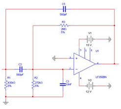
SPICE (Simulation Program with Integrated Circuit Emphasis) is an open source simulator which can be used to check the integrity of a circuit design and to check for errors. Usually this is done by visualizing the behavior of the circuit in a virtual environment, and it allows advanced analysis. Other simulators include PSpice and HSpice.
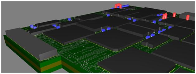
3: Board Layout
Once the schematic is complete, it is transferred to a board layout. Each symbol in the schematic has a land pattern. The land pattern is used to physically attach and electrically connect a component into a PCB. The land pattern translates the symbol of the component into an 8 pin rectangular package.In this stage the board outline is taken, the components are places and copper connections are made and finally the board is sent for fabrication.

4: Verification & Validation
One fabrication is complete, the board now needs to be validated. Prototype tests are usually involves which help to make sure the design meets the original specifications. Once validated, the prototype moves on to the product development stage.
Why Use Prototyping?
- Prototyping has a number of uses and can help to save a lot of time and money. For example,
- Prototyping is excellent for testing innovations that have a risk of failure and can help to rule out approaches that do not work beforehand.
- Prototyping will help to gather more accurate requirements before the project begins in case you have inadequate requirements.
- Prototyping helps to recognize and understand the technical problems in the design. Recognizing these problems will help to build a more accurate design.
- Prototyping helps to try several implementations of a feature and to analyze the result of each approach.
- People who develop prototypes are most likely to get funded as it helps to demonstrate the feasibility of the idea.
PCBGOGO Quick Turn PCB Fabrication and PCB Assembly Manufacturer


