
We classify PCBs into three types on the basis of the number of layers, single-sided, double-sided, and multi-layer. We can also classify them as flexible PCBs or rigid PCBs and flex-rigid PCBs. On the other hand if we classify them according to quality then we have three classes, Class1, Class 2 and Class 3. Class 3 is the most complex and these PCBs undergo the best inspection method. In this article we will discuss the quality inspection of rigid double-sided and multi-layered PCBs. Inspection is done to ensure the quality is up to mark and these are no errors or defects.

Inspection Standards:
PCB inspection can be categorized as the following types:
- PCB standards made by a country
- Military PCB standards by the military of a country
- PCB industrial standards (for e.g.SJ/T10309)
- Inspection for PCB standard quality set by device supplier
- Inspection for PCB requirement pre-labeled on PCB design drawings
PCB Inspection Items:
If we talk about the basic quality inspection methods then it is quite similar for all PCBs. The inspection can include visual inspection, electrical performance inspection, technological performance inspection and metalized via inspection.
? Visual Inspection:
Visual Inspection is done manually or automatically. The basic type involves the use of ruler, vernier caliper and magnifying glass. In visual inspection the board thickness, surface roughness and warpage is measured. The dimensions of assembly and their compatibility with electric connectors and lead rails is checked. The conductive traces of PCB are also inspected for clearness and integrity. Existence of bridging short circuit, open circuit, burr (raised edges), and voids are also checked.
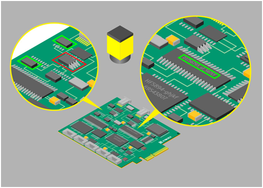
The PCB surface quality along with the inspection of any scratch or pin hole on traces or padding is done. The positions of the various vias are inspected, any missing vias are checked, their diameters according to design are also inspected. The quality of pad plating, firmness, roughness, brightness and various other factors are checked. The coating of PCB is also checked for quality along with even plating flux.
Electrical Performance Inspection:
When we talk about general electrical performance inspection, there are
two kinds of tests.

1: Connecting Performance Test: This test involves the use of a multimeter for inspection of connectivity of conductive traces specially the vias in double-sided PCBs and multi-layer PCBs.
2: Insulating Performance Test: This test is used to inspect the insulating performance of PCB by inspecting the insulating resistor used on the same place or between planes of the PCB.
? Technological Inspection:
This inspection involves checking the solderability and plating adhesion. Solderability is inspected by checking the performance of solder to conductice traces. Plating adhesion is inspected by sticking qualified tips to the plating plane and then pulling them off quickly after pressing. Plating plane is inspected for fall-off.
Metalized Via Inspection:
The quality of metalized vias is extremely important for double or multi-layer PCBs. Most problems usually arise due to low quality vias so it is important that the metalized via inspection is done properly. The via walls should not have empty holes or nodules and should be complete and smooth. The resistance change with environmental test should be over 5-10%. The adhesive intensity between metalized via and pad should be inspected .Metallographic analysis test is done to inspect the plating plane quality, thickness, uniformity, and adhesive intensity. Visual inspection and mechanical inspection are both involved here. In visual inspection the PCB is placed under a bright light source which is reflected evenly by the smooth walls of the via, unless a nodule or void disturbs the reflection.

Inspection of Multi-layered PCBs:


