




 日本語
日本語
 한국어
한국어

Smart Home PCB Design Solutions for Reliable Connected Devices
KEY DEFINITION
A smart home PCB is the physical platform that connects sensing, control, power and wireless communication inside a connected device. The right design depends on its power source, enclosure, radio, load and safety needs. A reliable solution also plans for assembly and testing before the first production order, not just for a working prototype.
A door sensor that misses an opening or a smart switch that drops off the network can make an otherwise polished product feel unreliable. In both cases, the problem may begin with a small decision on the circuit board: antenna placement, power routing or a test point left out of the layout.
This guide explains what a smart home PCB does, where different PCBAs are used, how sensor design changes the board, and what to ask a manufacturing partner before production.
What Is a Smart Home PCB
A smart home PCB is a printed circuit board designed for a connected household device; smart home PCBA means that board after its components have been mounted and soldered. Copper traces on the bare PCB connect the processor, power circuitry, sensors, radio and outputs. The finished PCBA becomes the device's electronic control center.
Consider a wireless temperature sensor. Its board may contain a sensor IC, microcontroller, antenna or radio module, battery circuit and programming pads. A smart plug has a very different layout: it must accommodate a power supply, switching device, connectors and the required separation between hazardous mains circuitry and user-accessible low-voltage circuits. Calling both products "smart home PCB" is accurate, but their design and test plans cannot be interchangeable.
Rigid FR-4 boards suit many switches, thermostats and hubs. Flexible circuits can route around a hinge, while rigid-flex combines stable component areas with a bendable connection.
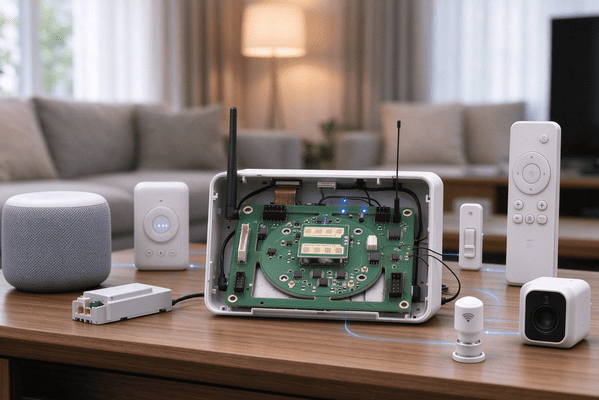
The Key Role of PCBs in Smart Home Automation
A smart home PCB turns a sensed event or user command into a dependable physical action. It gathers inputs, runs control logic, communicates with other devices and drives an output such as a relay, LED or motor. Those functions must keep working together during voltage dips, radio activity and changes in temperature.
Reliable power: A regulator and local decoupling keep the microcontroller stable when a radio transmits or a motor starts. For battery devices, sleep current matters as much as active current; measure the whole assembled board, not only a chip data sheet.
Clean signals: Ground return paths, sensor placement and separation from switching nodes help prevent noisy readings. A poor layout can turn a sound motion-sensing algorithm into repeated false triggers.
Useful connectivity: An antenna needs a manufacturer-specified keepout and a final-enclosure check. Thread Group describes Thread as an IEEE 802.15.4-based, IPv6 networking layer for low-power devices; the board still needs the correct radio and antenna implementation.
Safe actuation: Loads such as lamps, valves and locks need appropriate drivers, protection and thermal paths. Mains-powered designs also require a product-level safety review for the destination market.
Smart Home PCB and PCBA Applications
Smart home PCB and PCBA applications span devices that sense conditions, make decisions and control equipment. The end use determines whether the design priority is standby power, heat, radio performance, isolation or compact packaging.
Smart lighting: A wall dimmer or connected lamp combines control logic with an LED driver or switching stage. Heat near the driver and noise from fast switching deserve attention early in placement.
Security and access: A door lock may combine a battery supply, credential reader, motor driver and tamper input. Test the worst case during motor start, not just when the lock is idle.
Comfort and climate: Thermostats and air-quality monitors turn temperature, humidity or CO2 readings into HVAC actions. Keep sensing elements away from hot regulators and place enclosure vents where air can reach them.
Energy and automation: Smart plugs, blinds and irrigation controllers use sensing plus actuation to follow schedules or local conditions. Their boards must match the real electrical load and installation environment.
Types of Smart Home PCBA
Types of smart home PCBA are best grouped by the product function they support, since that function predicts the main design and test challenge. The table compares common, commercially relevant categories rather than suggesting that one board fits every device.
| PCBA type | Typical devices | Primary board concern |
|---|---|---|
| Lighting control | Smart bulbs, LED controllers, wall dimmers | Driver heat, dimming behavior, mains separation |
| Security and access | Smart locks, doorbells, cameras, alarms | Power peaks, tamper inputs, reliable communication |
| Home automation hubs | Gateways, control panels, voice hubs | Multiple radios, connectors, processing heat |
| Climate control | Thermostats, HVAC controllers, air monitors | Sensor accuracy and actuator isolation |
| Energy management | Smart plugs, meters, load controllers | Current sensing, switching heat, safety spacing |
| Motorized control | Blinds, curtains, garage controllers | Motor surge, position feedback, mechanical stress |
| Environmental sensing | Leak, smoke, occupancy, soil sensors | Low standby power, sensor exposure, false alarms |
| Appliance control | Connected washers, purifiers, kitchen devices | Load control, connectors, electrical noise |
Within each type, construction may be rigid, flexible or rigid-flex. A compact camera may need a multilayer board for dense processing, while a simple contact sensor can be smaller.
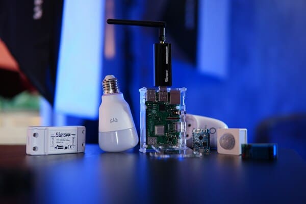
How Smart Home PCBs Support Sensor Applications
In sensor applications, the PCB determines whether a physical event reaches the controller as a trustworthy electrical measurement. Good sensor selection cannot compensate for a board that heats the sensing area, couples switching noise into an analog trace or blocks airflow.
For temperature and humidity, locate the sensor near the enclosure opening and away from warm processors or voltage regulators. For a passive infrared motion detector, preserve its optical field of view and keep noisy power circuitry away from its signal path. Leak sensors need corrosion-conscious exposed contacts and a way to verify detection after assembly; smoke or gas products require application-specific regulatory and calibration work beyond ordinary PCB assembly.
A practical prototype test uses the final housing, not only an exposed board. Record readings with the radio asleep and transmitting, with nearby loads switching, and at the intended mounting position. Compare repeated units as well as one "golden" sample. That simple matrix can expose self-heating, antenna shadowing and assembly variation before tooling and volume orders make corrections expensive.
For battery nodes, test wake-up current, transmit current and standby current across the full operating cycle. A sensor that sends one short alert but stays awake afterward may exhaust its battery despite a low advertised sleep specification.
Future Trends in Smart Home PCB Design
Smart home PCB design is moving toward broader interoperability, more sensing and tighter power budgets. Those trends affect the board's component selection and validation plan even when the external product looks unchanged.
Interoperable device categories: The Connectivity Standards Alliance added cameras, closures, soil sensors and expanded energy functions in Matter 1.5. Design teams should check whether their chosen chipset, memory, radio and test plan support the exact device features they intend to claim.
Lower power at the system level: More sensors will be expected to work for long periods between battery changes. That shifts attention from the microcontroller alone to leakage paths, wake circuitry, radio duty cycle and real firmware behavior.
More functions in small housings: Combining sensing, wireless, touch input and power conversion raises routing and thermal pressure. A multilayer stackup can help when a solid reference plane or tighter component placement is needed, but it adds cost and review work.
Security through the product life: Secure boot, protected credentials and update capability influence IC selection, programming steps and accessible test interfaces. Hardware security is a system design task, not a coating applied to a finished board.
How to Choose a Smart Home PCBA Manufacturer
Choose a smart home PCBA manufacturer by matching its verified process capabilities to your board and by agreeing on how each critical function will be tested. A low quote is useful only when it includes the work your device actually needs.
Check the process fit: Share the stackup, minimum features, package list, unusual connectors and assembly mix. Ask whether the supplier can build the required rigid, flex or rigid-flex format and handle both surface-mount and through-hole parts where needed.
Review inspection coverage: Ask what solder paste inspection, automated optical inspection and X-ray inspection will cover. Hidden-pad packages require a different inspection route from visible leads. Use IPC-A-610 acceptance criteria where appropriate, while remembering that visual acceptance does not prove product function.
Define functional tests: Specify pass or fail limits for radio pairing, sensor response, output switching and sleep current. Provide firmware, fixtures and a test procedure, then agree who records results and handles failed units.
Control the build package: Provide fabrication data, stackup, bill of materials with approved alternates, placement file, assembly drawings and polarity notes. Confirm component traceability, substitution approval and revision control before a pilot run.
Test the production path: Start with a small build, review defects and measurement spread, then lock the approved revision. Ask how first-article findings feed back into stencil, placement and test changes.
IPC identifies IPC-A-610 as an assembly acceptance standard and IPC-6012 as a rigid-board performance specification. Neither replaces the product safety, wireless and functional evaluations required for a specific smart home device.
How PCBgogo Supports Smart Home Projects
Smart home products often combine wireless modules, sensors, power circuits, processors and electromechanical components on the same assembly. PCBgogo provides an integrated manufacturing path that connects PCB fabrication, component sourcing, assembly, inspection and functional testing. This reduces coordination between multiple suppliers and helps keep the PCB, components and assembly data aligned under one revision.
Support from prototype to volume production: PCBgogo accepts orders starting from one piece, allowing engineering teams to validate a design before moving into pilot runs and larger production batches. Using the same manufacturing partner across these stages also makes production feedback easier to track and apply.
Broad PCB and assembly coverage: PCBgogo supports rigid, flexible and rigid-flex boards, together with SMT, through-hole and mixed-technology assembly. This is useful for smart home PCBAs that combine compact sensors and wireless ICs with relays, transformers, terminals or connectors that require stronger mechanical attachment.
Assembly for compact component packages: Its published capabilities include passive components down to 01005 packages, as well as BGA, micro BGA and QFN assembly. This supports space-constrained products such as smart locks, wireless sensors, control panels and connected cameras.
Inspection matched to assembly risks: Solder paste inspection checks the printing process before component placement, AOI identifies visible placement and soldering defects, and X-ray inspection examines hidden joints beneath BGA and QFN packages. Combining these methods provides more useful process coverage than relying on visual inspection alone.
Application-specific functional testing: PCBgogo can perform functional testing according to customer-provided procedures. For a smart home PCBA, the test plan may cover power-up behavior, wireless pairing, sensor response, actuator operation, firmware programming and current consumption in active and standby modes.
Defined workmanship requirements: PCBgogo lists support for IPC-A-610 Class 2 and Class 3 assembly requirements. The appropriate class and any additional product-specific acceptance criteria should be confirmed before production.
To receive an accurate quotation, provide the Gerber files, bill of materials, component placement file, assembly drawings and test instructions. Include the device’s power source, wireless protocol, enclosure constraints and critical operating limits so PCBgogo can evaluate the project against the required fabrication, assembly, inspection and testing processes.
PCBgogo - Reliable, High-Quality PCB Manufacturing
Save time and money with an all-in-one solution for PCB fabrication, assembly, and parts. Reduce vendor coordination, avoid split shipments, and get consistent, reliable quality.
Get Free Quote >
Conclusion
A successful smart home PCB design solution connects the electrical design to its enclosure, network, safety context and production test. Define the device's real operating conditions first, then choose the board format and manufacturing partner that can build and verify those conditions consistently.
Frequently Asked Questions
What is the difference between a smart home PCB and a smart home PCBA?
A smart home PCB is the bare board with patterned copper connections. A smart home PCBA is that board after components are mounted and soldered. The PCBA can be powered and tested as an electronic assembly.
Which PCB type is best for a smart home device?
The best type depends on the enclosure, component density and mechanical movement. Rigid boards suit many fixed products, while flex or rigid-flex can help in hinges and constrained housings. Select the stackup after mapping power, radio and sensor placement.
How does PCB layout affect wireless performance?
Layout affects antenna efficiency through ground geometry, nearby metal, noisy circuits and the enclosure. Follow the radio or module supplier's antenna keepout guidance, then verify range and pairing with the final housing installed.
What should be tested before smart home PCBA production?
Test the assembled device for power-up, radio pairing, sensor response, output control and current consumption in relevant operating states. Add safety, EMC and wireless compliance testing according to the product and sales region. A passing bare-board electrical test alone is insufficient.
Can one PCBA design serve every smart home product?
No single PCBA architecture fits lighting, battery sensors, cameras and mains-powered switches equally well. A reusable processor or radio module can shorten development, but power, sensing, actuation and safety layouts must fit the particular device.





