



 日本語
日本語
 한국어
한국어

PCB Layers: A Complete Guide to Types, Stackup, and How to Choose
Printed circuit boards (PCBs) are the backbone of virtually every electronic device — from smartphones and laptops to medical equipment and industrial machinery. At the heart of every PCB is its layer structure: a carefully engineered stack of conductive copper, insulating substrate, solder mask, and silkscreen that together allow electrical signals to travel precisely where they need to go.
Understanding PCB layers is essential whether you're a design engineer selecting a stackup, a procurement manager evaluating board costs, or a student just getting started in electronics. This guide covers everything — from what each layer does, to the differences between single-layer, double-layer, and multilayer PCBs, to how you determine the right number of layers for your project.
What Are PCB Layers?
PCB layers are the individual sheets of conductive and non-conductive material that are laminated together to form a complete circuit board. Each layer serves a distinct function: some carry electrical signals or power, while others provide insulation, mechanical support, or protection.
The total number of layers in a PCB directly determines its complexity, cost, and capability. Simple consumer electronics may use just one or two layers, while high-performance computing boards or RF devices can use 16 or more.
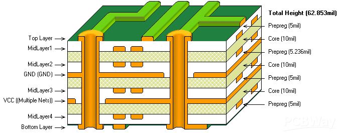
The Different Layers of a PCB: What Each One Does
Every PCB — regardless of layer count — is built from the same fundamental layer types. Here's what each one contributes:
1. Substrate (Core) Layer
The substrate is the foundation of any PCB. It is a non-conductive base material that provides mechanical rigidity and electrical insulation. The most widely used substrate material is FR-4, a glass-reinforced epoxy laminate valued for its excellent balance of electrical performance, thermal stability, and cost-effectiveness. High-frequency designs may use specialized materials such as Rogers or PTFE-based laminates with lower dielectric constants.
2. Copper Layer(s)
Copper layers are the electrically conductive pathways of the PCB. Thin sheets of copper foil are laminated onto the substrate, and a photolithographic etching process then removes the unwanted copper to leave behind the desired circuit traces, pads, and planes. Copper thickness is typically measured in ounces per square foot — standard boards use 1 oz copper (approximately 35 microns thick), while high-current power boards may use 2 oz or heavier copper.
Copper layers fall into two categories: signal layers, which carry data and control signals between components, and power/ground planes, which distribute power and provide a stable reference voltage while also helping with electromagnetic interference (EMI) shielding.
3. Solder Mask
The solder mask is a thin protective polymer coating applied over the copper traces on the outer layers of the PCB. It serves two primary purposes: it prevents accidental solder bridges during assembly, and it protects the copper from oxidation and environmental damage. The familiar green color of most PCBs comes from the solder mask — though blue, red, black, and white are also common options.
4. Silkscreen
The silkscreen is the outermost layer, printed on top of the solder mask. It contains human-readable information such as component reference designators (R1, C3, U5), polarity markings, manufacturer logos, and board revision numbers. The silkscreen does not affect electrical performance but is critical for assembly accuracy and field servicing.
Types of PCBs by Layer Count
The number of copper layers is the defining characteristic of a PCB's classification. Here is a comparison of the main types:
| Type | Copper Layers | Typical Applications | Relative Cost |
|---|---|---|---|
| Single Layer PCB | 1 | Simple electronics, LED lighting, power supplies | Lowest |
| Double Layer PCB | 2 | Consumer electronics, industrial controls, printers | Low–Medium |
| 4-Layer PCB | 4 | Smartphones, networking equipment, microcontrollers | Medium |
| 6–8 Layer PCB | 6–8 | High-speed computing, FPGA boards, automotive systems | Medium–High |
| Multilayer PCB (10+) | 10+ | Servers, RF/microwave, aerospace, medical imaging | High |
Single Layer PCBs
A single layer PCB (also called a single-sided PCB) has one copper layer on one side of the substrate. All components are mounted on the same side as the copper traces, making the design simple and the manufacturing cost very low. Single layer PCBs are ideal for uncomplicated circuits with low component density — think basic LED drivers, power adapters, remote controls, and simple sensor modules.
The main limitation is routing complexity: because all traces must exist on a single plane with no crossing allowed (without jumpers), single layer boards can only support relatively simple circuit topologies.
Double Layer PCBs
A double layer PCB (double-sided PCB) has copper on both the top and bottom sides of the substrate. The two layers are electrically connected through drilled and plated holes called vias. This dramatically increases routing flexibility and component density compared to a single layer board, at only a modest increase in cost.
Double layer PCBs are the most commonly used PCB type across consumer and industrial electronics. They strike the right balance between cost, capability, and manufacturability for the vast majority of designs — including Arduino-type microcontroller boards, motor drivers, and mid-complexity power electronics.
4-Layer PCBs
A 4-layer PCB adds two internal layers between the top and bottom copper layers. The typical 4-layer stackup dedicates the inner layers to a power plane and a ground plane, while the outer layers handle signal routing. This configuration delivers significant advantages: cleaner power distribution, reduced EMI, better signal integrity, and improved thermal performance.
The 4-layer PCB is the standard choice for designs involving high-speed digital signals, microprocessors, FPGAs, or mixed-signal (analog + digital) circuits. The dedicated ground plane acts as a return path for signals and provides shielding that is simply not achievable on a 2-layer board.
Multilayer PCBs
Multilayer PCBs contain 6 or more copper layers, with layers alternating between signal routing and power/ground planes. As layer count increases, designers gain more routing channels, better impedance control, and improved signal isolation between high-speed digital, analog, and RF sections.
High layer counts are found in complex applications such as server motherboards, telecommunications infrastructure, advanced driver-assistance systems (ADAS) in automotive, and medical imaging equipment. The tradeoff is cost and lead time: multilayer boards require more lamination cycles and tighter manufacturing controls.
PCB Layer Stackup: Why It Matters
The PCB layer stackup refers to the specific arrangement and sequence of all layers — copper, prepreg, and core — in a multilayer board. A well-designed stackup is not an afterthought; it is a fundamental part of the PCB design process that affects signal integrity, power integrity, impedance control, and EMI compliance.
Key principles of good stackup design include:
Symmetry: the stackup should be symmetric around the center to prevent warping during lamination.
Reference planes: every high-speed signal layer should be adjacent to a solid ground or power plane to control impedance and minimize crosstalk.
Power distribution: dedicated power planes should be closely paired with ground planes to form low-inductance power delivery networks.
Layer pairing: signal layers are typically paired with adjacent reference planes, and the distance between them (dielectric thickness) determines trace impedance.
How to Determine the Number of PCB Layers You Need
Selecting the right layer count is one of the earliest and most consequential decisions in PCB design. There is no universal rule — the right answer depends on your specific design requirements. Consider the following factors:
Component density: more components and tighter spacing require more routing layers.
Signal types: high-speed signals (USB 3.x, PCIe, DDR memory) demand controlled impedance and reference planes — typically a minimum of 4 layers.
Power requirements: designs with multiple voltage rails benefit from dedicated power planes.
EMI/EMC targets: if your product must pass FCC, CE, or similar regulatory testing, a 4-layer or higher stackup with proper ground planes is strongly recommended.
Budget: more layers increase board cost. Weigh the routing savings and performance benefits against the manufacturing cost difference.
As a general starting point: simple, low-frequency designs use 1–2 layers; microcontroller-based designs typically use 2–4 layers; high-speed digital and mixed-signal designs use 4–8 layers; and complex RF, server, or aerospace boards may use 10 or more layers.
Conclusion
PCB layers are the fundamental building blocks of modern electronics. From the single layer PCB powering a simple LED circuit to the 16-layer board inside a high-end network switch, each layer type — substrate, copper, solder mask, and silkscreen — plays a precise role in making electronic devices work reliably.
Understanding the different layers of a PCB, how they stack up, and how to choose the right layer count for your application gives engineers and product designers a critical advantage. Whether you're optimizing for cost with a 2-layer design or pushing performance with a complex multilayer stackup, the right layer strategy is the foundation of a successful PCB.





