




 日本語
日本語
 한국어
한국어

What Is a Power Bank Module? Power Bank Charger Circuit Board Guide
Key Takeaways
A power bank module combines charging, conversion, and protection. The battery alone cannot safely accept USB power or provide a regulated output.
PCB layout directly affects heat and voltage drop. Wide copper paths, short switching loops, thermal vias, and sound grounding improve efficiency and reliability.
FR 4 is the normal base material. Copper weight, glass transition temperature, laminate quality, and surface finish should match the current, temperature, and assembly process.
Price depends on the whole build. Layer count, board area, copper thickness, via structure, finish, component sourcing, inspection, and functional testing all change the quote.
Useful validation goes beyond checking a 5 V output. Test charge behavior, cutoff thresholds, load steps, connector heating, standby current, and repeated charge and discharge cycles.
Introduction
A power bank may look like a battery in a case, but a small electronic module largely decides its reliability. Excess heat, voltage drop, or poor load response can cause slow charging, resets, and faster cell aging.
This guide explains the complete power path and turns it into practical PCB choices for engineers, hardware startups, and purchasing teams evaluating a power bank charger circuit board.
What Is a Power Bank
A power bank is a rechargeable energy storage product that accepts electrical power, stores it in one or more cells, and later supplies a regulated output to another device. Most compact products use a single lithium-ion or lithium polymer cell group with a nominal voltage around 3.6 V or 3.7 V, while a USB output commonly requires 5 V or a negotiated higher voltage.
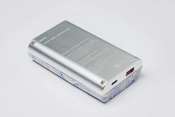
A power bank module is the assembled electronics between the cell and external connectors. A basic module includes charging, step-up conversion, battery protection, current sensing, and status control. Advanced versions add USB Type-C control, USB Power Delivery, fuel gauging, temperature sensing, or firmware.
How a Power Bank Works
A power bank works by managing energy through two operating paths: charging the cell from an external source and converting cell voltage into a controlled output for the load. The power bank charger circuit board decides which path is active, limits current, monitors temperature and voltage, and disconnects the battery when a protection threshold is reached.
During charging, the charger IC applies constant current, then holds constant voltage while current tapers. Voltage and current must match the selected cell limits. A design for a 4.20 V cell must not be reused with a different maximum charge voltage without review.
During discharge, a converter raises cell voltage to the requested output. A 10 W output at 5 V draws 2 A at the connector, while battery current is higher because cell voltage is lower and conversion has losses. Narrow traces or resistive connectors can therefore run hot.
The Role of the PCB in a Power Bank
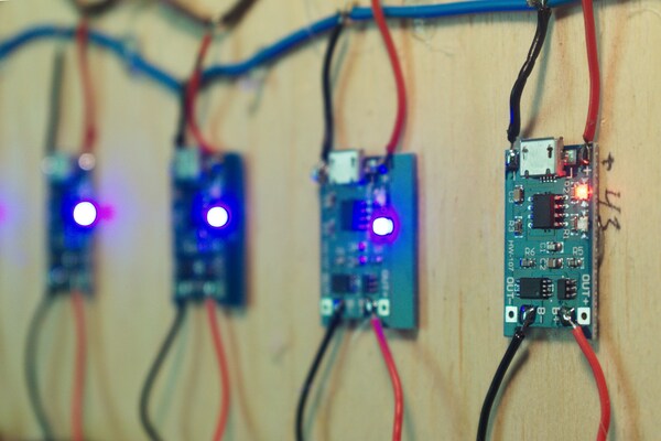
The PCB provides the electrical interconnection, current-carrying copper, thermal spreading, mechanical support, and controlled placement that allow the power management circuit to work as intended. In a compact module, layout is part of the circuit because parasitic resistance and inductance influence converter stability, electromagnetic noise, and protection response.
High current paths: Keep battery, MOSFET, inductor, sense element, and connector paths short and wide. Use copper pours and multiple vias between layers.
Switching loops: Place the input capacitor, switching IC, power devices, and inductor according to the IC reference layout to limit ringing and noise.
Thermal paths: Connect exposed pads to adequate copper and thermal vias, then measure temperatures inside the final enclosure.
Sensing and grounding: Keep voltage, current, and temperature sensing away from switching copper. Use Kelvin connections where current path drop would corrupt a measurement.
Mechanical interfaces: Support USB connectors with suitable shell tabs so cable insertion does not fatigue solder joints.
Choosing Materials for a Power Bank PCB
Power bank PCB materials should match current, heat, thickness, assembly temperature, mechanical stress, and cost. FR 4 suits many modules, but laminate grade and copper construction should not be left unspecified.
The following table summarizes practical choices for common designs.
| Design choice | Typical use | Engineering value | Watch point |
|---|---|---|---|
| FR 4 | Most rigid power bank modules | Good cost, availability, and multilayer support | Confirm laminate grade and Tg for the thermal profile |
| High Tg FR 4 | Hotter or denser assemblies | More margin against softening and z-axis expansion | It does not replace thermal analysis |
| 1 oz copper | Moderate current and compact prototypes | Common and economical | May need wider pours or more layers for low loss |
| 2 oz copper | Higher current power paths | Lower conductor resistance at the same width | Changes etching limits, spacing, and price |
| ENIG finish | Fine pitch pads and long storage needs | Flat solderable surface | Control pad design and avoid unnecessary finish cost |
| Lead-free HASL | Cost-focused boards with tolerant footprints | Economical and widely used | Surface is less planar for very small parts |
For many two-layer modules, 1 oz copper is adequate with wide pours and modest output power. Higher current products may justify 2 oz copper or added planes. Base the choice on calculated voltage drop and measured temperature rise.
Power Bank PCB Manufacturing Process
Manufacturing converts the approved design into a tested assembly through PCB fabrication, placement, soldering, inspection, and verification. Treating fabrication and assembly as one process helps manage interactions among copper geometry, pad finish, stencil design, and component tolerances.
File and DFM review: Check fabrication files, drill data, stackup, BOM, centroid data, polarity, and assembly drawings before material release.
Bare board fabrication: Imaging, etching, drilling, plating, solder mask, finish, routing, and electrical test create the PCB.
Solder paste and placement: Stencil apertures control paste volume, while placement data controls position and rotation. QFN thermal pads often need segmented apertures.
Reflow and secondary assembly: The thermal profile must suit the paste, laminate, and components. Through-hole connectors need a controlled soldering process.
Inspection and test: SPI checks paste, AOI checks visible assembly features, and X-ray can reveal hidden joints. Functional tests confirm power behavior.
What Determines Power Bank PCB Price
Power bank PCB price depends on board specifications, assembly complexity, components, test coverage, quantity, and schedule. A low bare board price can increase total cost if it causes delays, defects, or another prototype cycle.
Use the following cost map when requesting comparable quotes.
| Cost driver | Why it changes price | How to control it |
|---|---|---|
| Layer count and area | More material and process steps | Keep the outline efficient and add layers only when routing, heat, or EMI requires them |
| Copper and vias | Heavy copper and complex vias require tighter process control | Size power paths from calculations and avoid advanced vias without a density need |
| Surface finish | Different chemistry and handling costs | Match the finish to pitch, storage, and assembly needs |
| BOM and sourcing | IC availability, approved alternates, and order quantity affect cost | Provide manufacturer part numbers and controlled substitute rules |
| Inspection and test | Fixtures and test time add nonrecurring and unit cost | Define risks and measurable acceptance limits before quoting |
| Lead time | Expedited material and production slots can cost more | Freeze files early and separate prototype urgency from volume planning |
A complete RFQ should include board data, stackup, copper weight, finish, quantity breaks, BOM, placement data, drawings, firmware, and test instructions. Ask for separate tooling, component, fabrication, assembly, and testing costs.
How PCBgogo Helps Extend Power Bank Service Life
PCBgogo can help extend power bank service life by translating reliability requirements into controlled fabrication, assembly, inspection, and functional testing. Manufacturing cannot repair an unsafe schematic, but disciplined file review and process verification can prevent avoidable defects from being built into an otherwise sound design.
DFM review before production: Cross-checking files, BOM data, placement, polarity, and footprints can prevent rework and latent defects.
Controlled PCB construction: Material, plating, solder mask, finish, and electrical test affect current-carrying reliability. Put requirements on the fabrication drawing.
Assembly inspection: PCBgogo lists SPI, AOI, X-ray, visual inspection, and first article checks. Match the inspection plan to package and product risk.
Customer-defined functional testing: Tests can verify indication, output, standby current, load response, and protection behavior against agreed limits.
Send explicit acceptance criteria and retain test records by revision and lot so quality decisions remain traceable.
Why PCBgogo Is a Strong Partner for Power Bank PCB Projects
PCBgogo can coordinate PCB fabrication, sourcing, assembly, inspection, and testing in one workflow. This reduces file handoffs and provides one contact when power, thermal, or assembly issues cross process boundaries.
Quality coverage: Available controls include incoming and in-process checks, SPI, AOI, X-ray, visual QC, and customer-defined functional testing.
Prototype to production continuity: Support across order sizes lets a validated package and test method move forward without rebuilding the workflow.
Delivery support: Quick turn options can shorten prototype cycles when files are complete and materials are available. Final timing still depends on the build.
Engineering communication: Early questions about footprints, polarity, manufacturability, and test access reduce avoidable assembly risk.
One-stop execution: Coordinated fabrication, sourcing, assembly, inspection, and testing simplify accountability, revision control, and total cost tracking.
Submit a complete data package and request a documented manufacturing and test plan so PCBgogo can quote the actual power bank charger circuit board.
PCBgogo - Reliable, High-Quality PCB Manufacturing
Save time and money with an all-in-one solution for PCB fabrication, assembly, and parts. Reduce vendor coordination, avoid split shipments, and get consistent, reliable quality.
Get Free Quote >
Conclusion
A reliable power bank module depends on a matched cell strategy, correct power architecture, low-loss PCB layout, suitable materials, controlled assembly, and measurable testing. Before ordering, review the highest current paths, thermal conditions, connector mechanics, protection limits, and test access, then provide PCBgogo with a complete package for fabrication and assembly review.
Frequently Asked Questions
Is a power bank module the same as a battery protection board?
No. A protection board handles unsafe battery conditions, while a power bank module also manages charging and creates a regulated USB output. Integrated modules may combine both functions.
How many PCB layers does a power bank charger circuit board need?
Many basic modules use two layers, while four layers can improve grounding, density, heat spreading, and EMI control. Choose after placing the power stage and checking return paths.
Should a power bank PCB use 1 oz or 2 oz copper?
The correct copper weight depends on current, trace geometry, allowed voltage drop, temperature rise, and layer stackup. One ounce copper can work for modest loads with generous pours, while two ounce copper can reduce resistance when space or current makes one ounce impractical.
What files are needed for a power bank PCB assembly quote?
Provide fabrication data, drill files, stackup and notes, BOM with manufacturer part numbers, pick and place data, assembly drawings, and quantities. Include firmware, programming instructions, test procedures, acceptance limits, approved alternates, and any special packaging requirements when applicable.
How should a power bank PCB prototype be tested?
Test charging at the allowed input range, output regulation at several loads, startup, load steps, cutoff behavior, short circuit recovery, standby current, and connector temperature. Repeat critical tests at low and high battery states and inside the intended enclosure because airflow strongly affects temperature.
Can PCB manufacturing alone improve battery life?
Manufacturing quality can prevent excess resistance, weak solder joints, wrong components, and assembly defects, but battery life also depends on cell quality, charge voltage, temperature, discharge depth, firmware, and user load. Long service life requires both a sound design and consistent production.





