




 日本語
日本語
 한국어
한국어

PCB Connector Guide: Types, Pitch, Sizing and Selection
KEY DEFINITION
A PCB connector is a removable electrical interface between a printed circuit board and another board, cable, device, or power source. The right choice depends on what must connect, the space available, electrical load, assembly process, and how often the joint will be handled. Start with the mating interface, then check the exact part drawings and ratings.
An enclosure can have plenty of room for a circuit board and still fail to close because a cable exits its connector in the wrong direction. That is why connector selection belongs in the mechanical layout early, not at the end of the schematic.
What Is a PCB Connector?
A PCB connector makes an electrical connection that can usually be mated or unmated without soldering the two sides together. One side may be soldered or pressed into the PCB; the other may be a second board, a cable assembly, a battery, or an external plug. Contacts carry current or signals, while the housing positions those contacts and, in many designs, prevents incorrect mating.
The word connector describes the complete mating system, not just the plastic part visible on the board. A pin header needs a compatible receptacle. A wire-to-board header needs the correct housing and contacts. An FPC socket needs a cable with the specified thickness, contact orientation, and pitch. Two parts that look alike are not automatically a mating pair.
Connectors make assembly, replacement, and service easier, but each separable contact adds a possible point of resistance, wear, or intermittent connection. The aim is not to use the smallest connector available. It is to use the smallest system that meets the electrical, mechanical, and service requirements with margin.
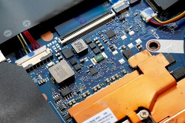
PCB Connector Types, Features, and Applications
PCB connector types are easiest to understand by what connects to the board. The tables below cover the common families used inside products and at their external interfaces. Some families overlap: a backplane connector is also a board-to-board connector, and a USB receptacle is also a board-mounted I/O connector.
1. Board-to-board and direct-contact connectors
These connectors join two PCBs or make contact with a board, module, or battery without a loose wire harness.
| Type | Defining feature | Common application | Watch for |
|---|---|---|---|
| Pin header and socket | Rows of exposed pins mate with a receptacle; straight and right-angle versions are common | Development boards, control modules, low-density daughterboards | A bare friction fit may need extra retention in vibration |
| Mezzanine or stacking connector | Two low-profile halves join parallel boards at a specified mated height | Compact instruments, cameras, embedded computers | Board spacing and alignment tolerances |
| Right-angle or coplanar board-to-board connector | Joins boards at 90 degrees or edge to edge | Daughtercards, modular control electronics | Insertion path and enclosure clearance |
| Backplane connector | High-position-count interface for cards that plug into a shared board | Servers, telecom shelves, industrial racks | Guide hardware, insertion force, and signal integrity |
| Card-edge socket | Spring contacts grip plated fingers on a PCB edge | PCIe cards, M.2 modules, memory modules | Board thickness, keying, finger geometry, and finish |
| Spring contact, pogo pin, or battery contact | Spring-loaded metal contact meets a flat pad or battery terminal | Charging docks, removable batteries, test fixtures | Compression travel, pad wear, and alignment |
Card-edge connectors deserve one distinction: the socket is a connector, while the mating "gold fingers" are features made on the PCB itself. Their bevel, thickness, plating, and position must match the socket drawing. A footprint alone cannot guarantee a fit.
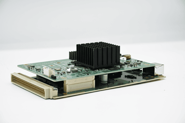
2. Cable-to-board and power connectors
These families bring power or signals from wires, ribbon cables, or flexible circuits onto the PCB.
| Type | Defining feature | Common application | Watch for |
|---|---|---|---|
| Crimp wire-to-board system | Individual wire contacts lock into a housing that mates with a PCB header | Fans, sensors, motors, appliance harnesses | Correct crimp tool, wire gauge, terminal retention, and mating series |
| IDC or ribbon-cable connector | Contacts displace insulation across several conductors at once | Internal flat-cable links and legacy equipment | Cable pitch, conductor order, strain relief, and polarization |
| FFC/FPC connector | Low-profile socket accepts flat flexible cable or flexible printed circuit | Displays, cameras, laptops, compact controls | Cable thickness, exposed-contact side, actuator style, and bend radius |
| PCB terminal block | Screw, spring, or push-in clamp accepts field wiring | Industrial I/O, power supplies, building controls | Wire preparation, torque or actuation method, voltage spacing |
| Pluggable terminal block | Removable wired plug mates with a PCB-mounted base | Serviceable industrial controls | Plug/base compatibility and full seating |
| Board-in or direct-wire contact | Wire contact terminates directly in or at the PCB, sometimes without a separate board header | High-volume appliances and lighting | Process tooling and whether the joint is intended to be removable |
| High-current power connector | Larger contacts, blades, or multiple parallel contacts carry power | Battery packs, power distribution, server power | Temperature rise, current sharing, and cable strain |
An FFC/FPC socket is especially useful when height matters, but "0.5 mm pitch" does not describe the complete interface. Molex lists FFC/FPC connector pitches from 0.20 to 2.00 mm across its portfolio, with different actuator and circuit-count options. The exact cable specification still decides compatibility.
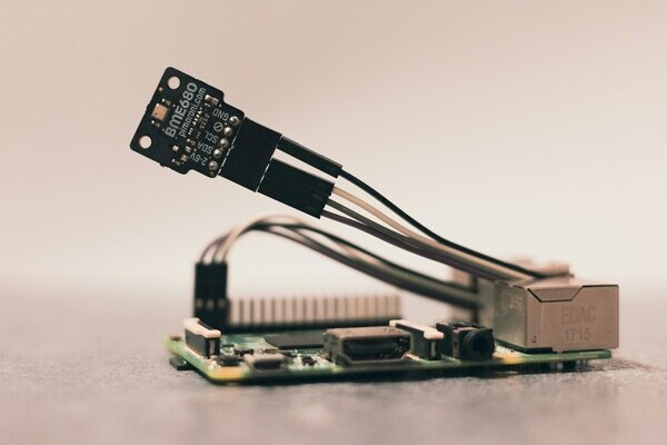
3. Board-mounted external and specialized interfaces
These are chosen partly by the device or cable on the other side, so the interface standard matters as much as the PCB footprint.
| Type | Defining feature | Common application | Watch for |
|---|---|---|---|
| USB receptacle | Standardized external data and power interface | Charging, peripherals, service ports | Shell anchoring, pinout, and supported protocol or power mode |
| HDMI or DisplayPort receptacle | Dense external video interface | Monitors, cameras, media equipment | Shield connection, differential-pair routing, and insertion stress |
| Modular jack, often called RJ45 | Latching modular plug interface, sometimes with integrated magnetics | Ethernet equipment | Jack configuration, magnetics, LED pins, and panel opening |
| D-sub connector | Metal-shelled multipin interface, often with jackscrews | Industrial serial I/O and legacy instruments | Shell grounding and panel hardware |
| RF coaxial connector | Controlled-impedance center and shield contact | Antennas, RF modules, test equipment | Impedance, launch layout, torque or snap-cycle limits |
| Circular or sealed PCB connector | Keyed shell, often with a latch or coupling thread | Outdoor sensors, vehicles, harsh environments | Whether the mated system achieves the required ingress rating |
| Storage or module connector | Form-factor-specific socket such as SATA, M.2, or a memory-card socket | Drives, wireless modules, removable media | Standard revision, key position, card retention, and board space |
Connector terminology is often used too loosely. A familiar label may describe an entire product family, an interface format, or simply a similar housing shape, even though the parts differ in pitch, keying, contact orientation, or pin assignment. When sourcing a replacement, verify the product series, part number, mechanical drawing, and specified mating component instead of relying on appearance or a generic nickname.
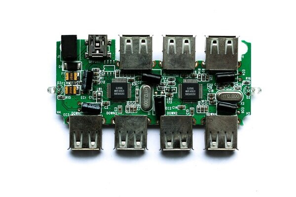
Common Features of PCB Connectors
Every PCB connector combines an electrical contact, a mating geometry, and a way to attach to the board. The useful comparison is how those details behave in your actual product, rather than how many pins the connector has.
Electrical rating. Check current per contact, rated voltage, contact resistance, and temperature rise under the conditions specified by the manufacturer. Do not assume that ten contacts rated at 1 A each create a 10 A power path. Current sharing depends on pin assignment, trace geometry, contact resistance, and the manufacturer's derating rules.
Contact system. Many signal contacts use a copper alloy with tin or gold plating. The finish affects mating behavior and corrosion performance, but plating alone does not define durability. Check the specified mating cycles and whether the design is meant to be disconnected during routine service.
Retention and error prevention. Friction, latches, screws, guide posts, and positive locks keep a connection engaged. Keying and polarization reduce wrong-way assembly. A latch helps only if the harness has enough slack that a tug does not load the solder joints.
Environmental and signal performance. Housings have temperature limits; some connector systems also provide sealing or shielding. For fast signals, the connector, board launch, return path, and cable form one channel. A connector advertised for high speed cannot correct poor routing on either side.
Board termination. Surface-mount, through-hole solder, and press-fit versions can exist within one connector family. Choose the version that suits both the mechanical loading and the factory process. They are not interchangeable footprints.
PCB Connector Pitch and Size
Connector pitch is the center-to-center distance between adjacent contacts in the same row. It determines contact density, but it does not tell you the connector's total width, height, board footprint, or mating clearance. For a single straight row, the span from the first contact center to the last is (number of positions ? 1) × pitch. A 10-position row at 2.54 mm pitch spans 22.86 mm between those centers; the plastic body extends beyond that span.
The following are useful starting points, not universal ranges or substitutes for a selected part drawing.
| Example pitch | Where you may encounter it | What the number does not tell you |
|---|---|---|
| 0.30 or 0.50 mm | Dense FFC/FPC sockets and some fine-pitch board connectors | Cable thickness, contact side, and latch style |
| 1.00 or 1.27 mm | Compact signal headers and wire-to-board systems | Current rating and mating height |
| 2.00 or 2.54 mm | General-purpose headers and some harness connectors | Pin length, row spacing, and retention |
| 3.50 or 5.08 mm | Some PCB terminal blocks | Voltage rating, wire size, or required clearance |
For example, Phoenix Contact specifies a 5.08 mm pitch for one push-in PCB terminal block, but its datasheet also gives the hole diameter, installed height, wire range, and rating conditions. That is the level of detail needed before layout release.
Check the mated height for stacked boards, the unmated height for assembly access, and the cable exit direction for enclosures. Also compare PCB thickness, finished hole size, pad pattern, keepout, and insertion/removal path against the mechanical model. A smaller pitch helps only when the resulting assembly can still be built, inspected, and serviced.
PCB Connector Installation and Maintenance
Reliable installation starts with the manufacturer's drawing and processing instructions for the exact part number. Similar-looking variants may change the recommended land pattern, cable insertion direction, reflow limit, or application tooling.
Confirm the complete mating pair. Match the series, position count, pitch, keying, contact finish, cable specification, and any required secondary locks before releasing the bill of materials.
Place the connector for access. Leave space for fingers or tools to operate the latch, for the cable's bend radius, and for the mating part's full insertion path. Add board support or mounting hardware where repeated plug force could flex the PCB.
Build the correct footprint. Use the manufacturer's recommended pads or finished plated-hole dimensions. Check the 3D body and pin-one orientation against the board edge and enclosure opening.
Use the specified assembly process. Solder surface-mount and through-hole variants to their stated profiles. For press-fit parts, control the finished hole and use the prescribed support and insertion tooling. TE describes compliant press-fit contacts as a solderless connection whose performance depends on both the pin and plated through-hole.
Inspect the finished joint. Check solder wetting or press-fit seating, housing damage, bent contacts, and latch engagement. On a harness, verify crimp height or pull requirements using the terminal manufacturer's process specification.
Test in the intended operating state. Verify continuity and polarity, then check voltage drop or temperature rise under realistic load. For high-speed links, use the applicable channel test rather than continuity alone.
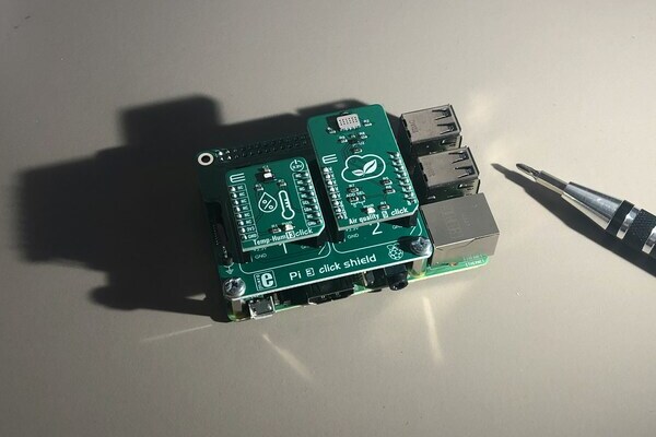
During service, disconnect power before touching the assembly. Release latches using their intended actuator, pull on the plug body rather than the wires, and inspect for discoloration, corrosion, bent pins, cracked housings, or loose board joints. Clean contacts only with a method approved for that connector; aggressive scraping can remove plating. If a contact is worn or heat damaged, replacement is usually more dependable than bending it back into shape.
Turn Your PCB Design Into a Fully Assembled Product
Stop coordinating separate suppliers for PCB fabrication, component sourcing, connector installation, and final assembly. PCBgogo brings the entire process into one manufacturing workflow, reducing handoffs, communication delays, and unexpected production costs.
Why work with PCBgogo?
One-stop PCB production: Move from PCB fabrication and component sourcing to SMT, through-hole, and mixed-technology assembly with one supplier.
Connector assembly support: Install fine-pitch FPC sockets, board headers, terminal blocks, power connectors, and other supported connector types during PCBA production.
Flexible sourcing options: Choose full turnkey, partial turnkey, or consigned assembly based on your BOM and supply-chain requirements.
Cable and product integration: Add custom cable assemblies, wiring harnesses, hardware installation, and optional enclosure assembly.
Inspection and testing: Combine component inspection, assembly inspection, electrical testing, and final delivery within the same production workflow.
Lower coordination costs: Reduce repeated quotations, split shipments, supplier handoffs, and responsibility disputes.
PCBgogo - Reliable, High-Quality PCB Manufacturing
Save time and money with an all-in-one solution for PCB fabrication, assembly, and parts. Reduce vendor coordination, avoid split shipments, and get consistent, reliable quality.
Get Free Quote >
PCB Connector Challenges and Solutions
Most connector failures come from a mismatch between the selected part and the conditions around it. The symptoms below provide a practical first check, though a root cause still needs inspection and measurement.
| Symptom or challenge | Likely cause to investigate | Practical response |
|---|---|---|
| Intermittent connection after vibration | Insufficient retention, fretting, cable movement, or cracked solder joints | Choose a locking system, add strain relief, support the PCB, and test the assembled product under vibration |
| Warm connector or browned housing | Contact resistance, overload, incomplete mating, or undersized board copper | Measure voltage drop and temperature rise at rated load; review current derating, crimp quality, and full current path |
| FPC works only when pressed down | Cable not fully inserted, wrong contact orientation, damaged actuator, or wrong cable thickness | Verify the exact cable and socket drawings; replace a broken latch instead of wedging the cable |
| Plug fits but pins map incorrectly | Similar housings from different series, reversed view of pinout, or missing keying | Compare both mating drawings from the same viewing direction and add assembly inspection points |
| High-speed link fails despite continuity | Impedance discontinuity, poor return path, excess stub, or damaged shield termination | Review the connector launch, layer transition, grounding, and complete cable channel |
| Connector tears pads or flexes the board | Repeated insertion load borne by solder joints | Use mounting tabs, through-hole anchors, panel support, or a lower-force interface |
| Sealed product admits moisture | Seal omitted, wrong cable diameter, or enclosure opening outside the specified fit | Verify the complete mated and mounted system, including gasket compression and cable entry |
One selection habit prevents many of these problems: specify the connector and its mate as a system on the drawing or bill of materials. Include the cable, contacts, tooling, PCB geometry, and enclosure fit where they affect function. Then validate a physical prototype before treating a catalog rating as proof that the full assembly works.
Conclusion
Choose a PCB connector by the connection it must make, then confirm its electrical rating, pitch, mating geometry, retention, and assembly method from the exact product documentation. A quick prototype fit check and a loaded electrical test will catch more problems than choosing from pitch or pin count alone.
Frequently Asked Questions
What is the difference between a PCB connector and a terminal block?
A PCB terminal block is one type of PCB connector. It clamps individual wires with a screw, spring, or push-in mechanism; other PCB connectors mate with housings, cables, boards, batteries, or standardized external plugs.
Does a smaller PCB connector pitch always save space?
No. A finer pitch reduces contact spacing, but the actuator, housing, cable bend, mounting hardware, and required service clearance may control the final space claim. Compare the full mated 3D envelope, not pitch alone.
Are PCB connectors with the same pitch interchangeable?
No. Equal pitch does not guarantee matching pin dimensions, contact orientation, housing shape, keying, voltage rating, or plating. Verify the manufacturer's specified mating part numbers.
Which is better for a PCB connector: surface mount or through-hole?
Neither is universally better. Surface mount suits automated assembly and compact layouts; through-hole or mechanically anchored parts can help manage higher insertion loads. The correct choice depends on the connector design, board support, and manufacturing process.
Can a PCB connector carry more current if several pins are paralleled?
Sometimes, but only if the manufacturer permits it and the layout shares current predictably. Check total temperature rise, contact derating, trace and cable capacity, and the consequences of one pin failing to mate.
How do I identify an unknown PCB connector for replacement?
Start with the number of positions, measured center-to-center pitch, row count, mating direction, latch or key shape, and any molded marking. Then compare the full mechanical drawing and mating-part list; appearance and pitch by themselves are not enough.





