日本語
 한국어

PMOS vs NMOS for PCB Design and Power Switching
QUICK ANSWER Choose an NMOS for a ground-side switch or when low loss matters most. A P-channel device suits a simple positive-rail switch at modest current. A high-side N-channel device can be more efficient, but its gate needs a driver that raises it above the source voltage. In every case, verify the available gate drive, body-diode direction, heat, and PCB current path before releasing the board.
A load switch that works on the bench can still overheat or power a load while "off." The schematic symbol is only the start: gate voltage, package heat flow, and copper layout determine whether the assembled PCB behaves as intended.
KEY TAKEAWAYS1. Pick the switch position first: low side is usually easiest with an N-channel device; high side is simpler with a P-channel device.2. Compare RDS(on) at the actual gate-source voltage and hot operating temperature, not at the threshold voltage.3. Check the body diode and default gate state, then size copper and vias for the expected loss.
Understanding NMOS and PMOS Transistors
Both are voltage-controlled MOSFETs with gate, drain, and source terminals. For the enhancement-mode power devices commonly used on PCBs, the N-channel type turns on when its gate is sufficiently positive relative to its source; the P-channel type turns on when its gate is sufficiently negative. "Sufficiently" means the voltage used for the specified RDS(on), not merely the VGS(th) value where conduction begins.
Structural Differences Between NMOS and PMOS
An NMOS conducts mainly through electrons in an n-type channel; a PMOS uses holes in a p-type channel. Electron mobility is higher, so comparable silicon area generally gives the N-channel device lower on-resistance. The intrinsic body diode also points in the opposite direction. Check the actual device pinout and diode orientation in the datasheet before assigning PCB pads; a reversed source and drain may leave an unintended current path.
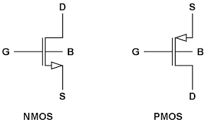
How NMOS and PMOS Work in a Circuit
For a low-side NMOS, connect source to ground and drain to the load. A gate drive above ground creates positive VGS. For a high-side PMOS, connect source to the supply and drain to the load; pulling the gate below the supply creates negative VGS, while pulling it back to the source turns it off. If a controller cannot tolerate the supply voltage, use a suitable level shifter rather than connecting its pin directly to the gate.
The source of a high-side N-channel switch rises as it turns on. Its gate must remain above that source by the drive voltage required for the specified RDS(on), typically using a high-side driver. Also keep |VGS| within the device rating in every operating state, including startup and transients.
PMOS and NMOS Pros and Cons
| Choice | Main advantage | Main trade-off |
|---|---|---|
| Low-side NMOS | Simple ground-referenced drive; low conduction loss | Disconnects ground, so the load may still sit at supply potential |
| High-side PMOS | Simple positive-rail switching | Often higher RDS(on) for similar die size; check gate voltage limit |
| High-side NMOS | Low loss at higher current | Needs a suitable driver and extra layout attention |
NMOS and PMOS Applications on a PCB
Use NMOS for ground-side LED, solenoid, or motor control when switching the return path is acceptable. Use PMOS for a compact high-side sensor or peripheral power switch when its voltage drop and dissipation fit the budget. For a high-current rail, compare the two options using P ≈ I2 × RDS(on) at operating temperature; switching loss also matters under PWM.
Before fabrication, place the MOSFET close to the load or rail connection, keep the high-current loop short and wide, and provide copper and thermal vias according to the package's heat path. Put the gate resistor near the gate, add a gate-to-source resistor for a defined off state, and verify that the trace and connector ratings match the load current. For inductive loads, include the required flyback path. A single MOSFET body diode may prevent true bidirectional isolation; use a suitable back-to-back arrangement if that is required.
FAQ
Can I swap the two types in the same PCB footprint?
Usually not directly. Gate polarity, drive circuitry, body-diode direction, and sometimes pinout change.
Does a logic-level device always work from a 3.3 V GPIO?
Only if its RDS(on) is specified at a gate voltage your GPIO can deliver and the pin can charge the gate fast enough for the switching rate.
Which is better for battery-powered boards?
For low current, a P-channel high-side switch may save driver parts; at higher current, N-channel efficiency may outweigh the driver cost. Compare total loss and quiescent current.