日本語
 한국어

What is MOSFET Transistor? A Practical PCB Guide
QUICK ANSWER A MOSFET transistor is a voltage-controlled switch whose gate changes the current path between the drain and the source. For PCB designers, the useful questions are whether the available gate drive fully enhances it, where the body diode conducts, how much heat the copper must remove, and whether the layout keeps switching loops short.
A MOSFET transistor that works on the bench can still overheat or ring on a production PCB. The usual causes are a marginal gate voltage, an unintended diode path, or copper and routing that do not match the switching current. This guide follows MOSFET transistor decisions from schematic to layout.
What Is a MOSFET?
MOSFET means metal-oxide-semiconductor field-effect transistor. Its insulated gate draws little steady-state current, but charging and discharging that gate takes current during switching. A MOSFET transistor has gate (G), drain (D), and source (S) terminals; most discrete power devices also have an internal body connection tied to the source. Always confirm the actual package pinout and exposed-pad connection in the chosen datasheet.
How a MOSFET Works
Gate-to-source voltage, VGS, creates or removes a conductive channel. In a common N-channel enhancement MOSFET transistor, a positive VGS turns the channel on; a P-channel version needs negative VGS. Gate threshold, VGS(th), marks the onset of conduction at the datasheet's small test current. It does not mean the device is fully on. For switching, check RDS(on) at the lowest gate-drive voltage your circuit will actually provide, including startup and supply tolerance.
The gate is capacitive. A driver must move the MOSFET transistor's gate charge each cycle, so a low RDS(on) part with high gate charge may run hotter at high frequency than expected. Estimate conduction loss with I2RDS(on), then include switching loss and the rise of RDS(on) with junction temperature.
MOSFET Characteristics That Matter on a PCB
| Check | PCB Decision |
|---|---|
| VDS and transients | Rate the device above the highest drain-source voltage, including switching overshoot. |
| RDS(on) at VGS | Use the specified value at your real gate drive and hot operating condition. |
| Gate charge and capacitance | Size the driver and keep the gate-drive path and its return close together. |
| Thermal path | Provide copper area and thermal vias as the package guidance requires; verify temperature on the assembled board. |
Before releasing the PCB, compare the MOSFET transistor datasheet conditions with the actual supply, current, gate drive, switching frequency, and ambient temperature. Inspect the footprint's pad numbering and exposed-pad net in the CAD library. On the first assembled board, measure VGS at the package pins and drain overshoot during the worst load transition. These checks catch errors that a nominal current rating cannot reveal.
MOSFET Types
Channel polarity and default state define four MOSFET transistor types. Enhancement types are normally off at VGS = 0; depletion types are normally on. Most board-level power switches use enhancement devices, while depletion parts appear in specialized startup or current-limiting circuits. The four simplified sketches below show channel state, not package pins or body diodes.
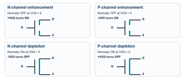
Choose an N-channel enhancement MOSFET transistor for a simple low-side switch when its lower on-resistance is useful. A P-channel enhancement MOSFET transistor can simplify a modest-current high-side switch, but its gate must be driven below its source. N-channel high-side switching generally needs a driver that can raise the gate above the source.
Lateral and Vertical MOSFET Structures
In a lateral MOSFET transistor, current mainly travels along the silicon surface; this suits many signal and integrated-circuit devices. In a vertical power MOSFET transistor, current travels through the die thickness, allowing a larger effective channel area and a backside drain connection. For PCB assembly, that backside drain often reaches an exposed pad or tab. Treat it as an electrical node when assigning copper and heatsinking, especially if the tab could contact a chassis.
MOSFET Biasing
Biasing sets VGS and VDS in the intended operating region. For an N-channel low-side MOSFET transistor switch, source goes to ground, load goes between supply and drain, and a defined gate pulldown keeps the MOSFET transistor off during reset. Put a small gate resistor near the gate if ringing demands it; choose its value from measured turn-on and turn-off behavior. For inductive loads, provide a deliberate current path when the switch opens and check the clamp's voltage and energy rating. A high-side MOSFET transistor design needs its own gate-drive and startup check.
Common Mistakes When Reading MOSFET Symbols
First, do not infer MOSFET transistor pin numbers from a schematic symbol: the footprint and datasheet pin map control assembly. Second, the arrow identifies channel type in many symbol conventions, while the broken or solid channel denotes enhancement or depletion mode; symbol styles vary, so read the device label. Third, a MOSFET transistor's intrinsic body diode can conduct with the gate off. Check its direction before using a single device for reverse-current blocking or bidirectional isolation. Back-to-back devices may be needed.
MOSFET vs BJT
A MOSFET transistor is driven by gate voltage and gate charge; a BJT needs continuing base current to stay on. A fully enhanced MOSFET's conduction loss is approximately I2RDS(on), while a saturated BJT's is approximately IC × VCE(sat). Neither is universally better: compare loss, drive complexity, voltage rating, switching speed, and heat at the actual operating point. On a PCB, the MOSFET's fast edges make loop inductance and gate routing especially important.
Frequently Asked Questions
Can a 3.3 V MCU pin drive a MOSFET directly?
Only if the datasheet specifies adequate RDS(on) at the available VGS and the MCU can charge the gate fast enough. Check startup, PWM frequency, and gate current rather than relying on VGS(th).
Why is my MOSFET transistor hot despite a low RDS(on)?
The part may have insufficient VGS, significant switching loss, inadequate copper, or a high-temperature RDS(on). Measure gate and drain waveforms at the device and check the thermal path.
How should the MOSFET transistor be placed on the PCB?
Keep the high-current loop compact, place the driver close to the gate, and route the gate return beside the drive trace. Follow the package's copper and via recommendations, then confirm the layout with temperature and waveform measurements.