



 日本語
日本語
 한국어
한국어

PCB DFM: How to Prevent Manufacturing Issues Before Production
A PCB layout can pass every rule check in your design software and still fail the moment it reaches a fabrication line. Design for Manufacturability (DFM) is the step that closes that gap — it checks your board against the physical and process limits of the equipment that will actually etch, drill, plate, and assemble it. This guide covers what DFM in PCB design means, why is DFM important for PCB board design, the specific PCB DFM guidelines engineers check before releasing files, and how to build a DFM review into your workflow so problems get caught on screen instead of on the production floor.
What Is DFM in PCB Design?
DFM in PCB design is a structured check of a layout against the manufacturing and assembly capabilities of the shop that will build it. Where Design Rule Checking (DRC) inside your CAD tool confirms that a layout matches the constraints you programmed into the software, DFM asks a broader question: can this board actually be built reliably, at a reasonable cost, with the equipment and processes available? That includes two sides of production:
Fabrication-side DFM: copper etching tolerances, drill and plating limits, solder mask registration, and panelization.
Assembly-side DFM: component footprint accuracy, placement spacing for pick-and-place equipment, solderability, and test access.
A board can pass DRC cleanly and still fail DFM — for example, a trace routed at a sharp angle can meet every spacing rule in the software while still creating an acid trap that a fabricator's etching bath cannot handle cleanly.
Why Is DFM Important for PCB Board Design?
The core reason DFM matters is timing: the earlier a design flaw is caught, the cheaper it is to fix. A pad clearance issue found during a DFM review is a five-minute layout edit. The same issue found after a board has already been fabricated and assembled means scrapped material, a re-spin, and a delayed schedule. This pattern holds up consistently across the industry — the further a flaw travels down the production line before it's caught, the more expensive it becomes to correct.
| Stage a Flaw Is Caught | Typical Relative Cost to Fix |
|---|---|
| DFM review, before fabrication | Baseline |
| First prototype / first-article build | Several times baseline |
| Volume production run | Tens of times baseline |
| After field deployment | Highest — includes rework, shipping, and reputational cost |
Beyond cost, a solid DFM process delivers a few compounding benefits:
Higher yield. Boards designed within a fabricator's real process window come off the line with fewer shorts, opens, and solder defects, so fewer units are scrapped or reworked.
Shorter lead times. A design that doesn't need a re-spin moves straight from Gerber submission to production, avoiding the days or weeks a correction cycle adds.
Better long-term reliability. Issues like uneven thermal relief or marginal annular rings often don't fail immediately — they show up as intermittent faults or early field failures months later. DFM catches these before they ship.
Lower total cost. Fewer re-spins and higher yield offset the small amount of time a DFM review adds to the design cycle, so the net effect on budget is almost always positive.
PCB DFM Guidelines: The Core Design Rules to Check
These are the design rules that come up most often in a DFM review, organized by the part of the board they affect.
Trace Width and Spacing
Every fabricator has a minimum trace width and spacing (often expressed as, for example, 6/6 mil for standard boards or tighter for advanced HDI processes). Traces routed thinner than the process allows risk being over-etched into an open circuit; traces spaced too closely risk bridging. Route corners at 45 degrees or with curves rather than sharp right angles — acute-angle corners trap etching chemical and erode the trace faster than the rest of the run.
Via Size, Drill, and Annular Ring
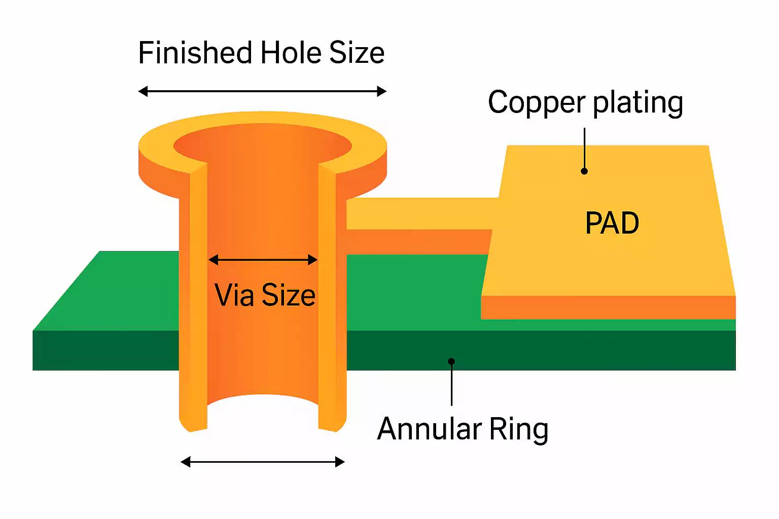
Drill bits have physical limits, commonly expressed as an aspect ratio (board thickness divided by hole diameter); a 10:1 ratio is a widely used safe ceiling for standard fabrication. Just as important is the annular ring — the ring of copper around a drilled hole. If it's too thin, ordinary drill wander during manufacturing can break the ring and sever the connection, an issue known as drill breakout.
Component Placement and Courtyard Clearance
Components need enough clearance from each other for a pick-and-place nozzle to set them down without disturbing a neighboring part, and enough room afterward for rework tools or a soldering iron to reach the pins. Checking 3D courtyards during layout — not just 2D silkscreen outlines — catches tall components that would otherwise physically collide.
Solder Mask Clearance and Webbing
Solder mask needs a small expansion around each pad to allow for registration tolerance during printing. Too little expansion and the mask can creep onto the pad, blocking solder; too little mask webbing between fine-pitch pads invites solder bridging during reflow.
Copper Pour and Thermal Relief
Connecting a component pad directly to a large copper plane turns that plane into a heat sink during reflow, pulling heat away from the joint faster than the surrounding pads heat up. This produces cold or dry joints on components that are otherwise correctly placed. Thermal relief spokes — thin copper connections between the pad and the plane — solve this without materially affecting the plane's electrical performance.
Board Edge and Panelization Clearance
Traces and components near a board edge or a V-score line are exposed to mechanical stress during depanelization. A keep-out zone along all edges — commonly in the range of 50 to 100 mils — protects components (especially brittle ones like multilayer ceramic capacitors) from cracking when boards are separated from the panel.
Common DFM Issues at a Glance
| Issue | What Causes It | How to Prevent It |
|---|---|---|
| Acid trap | Traces routed at a sharp, acute angle | Route corners at 45° or with curves |
| Drill breakout | Annular ring too thin for the fabricator's drill tolerance | Increase pad size relative to drill diameter |
| Solder bridging | Insufficient pad spacing or mask webbing | Follow the fabricator's minimum spacing and mask expansion rules |
| Tombstoning | Uneven thermal mass on a two-pad passive component | Balance copper connections on both pads of the component |
| Cold or dry joints | Pad tied directly to a large copper pour | Use thermal relief spokes instead of a direct flood connection |
| Cracked components | Brittle parts placed too close to a board edge or V-score | Keep a clear zone near edges and depanelization lines |
| Blocked test access | Test points placed too close to tall components | Maintain clearance around test points for probe access |
DFM vs. DRC: What's the Difference?
These two checks are related but answer different questions, and a board can pass one while failing the other.
| Aspect | DRC (Design Rule Check) | DFM (Design for Manufacturability) |
|---|---|---|
| What it checks | Whether the layout obeys the rules programmed into the CAD software | Whether the board can actually be built and assembled reliably |
| When it runs | Continuously, inside the design tool | Before Gerber files are released for production |
| Example catch | Trace spacing below a programmed limit | A trace that meets spacing rules but forms an acid trap |
PCB DFM Checklist Before You Submit Gerber Files
Run through this list before generating and submitting your manufacturing files:
Trace-to-trace, trace-to-pad, and pad-to-pad clearances meet the fabricator's minimum spacing.
Smallest drill size stays within the fabricator's maximum aspect ratio, with adequate annular rings on all vias.
Component courtyards checked in 3D — no physical overlap and enough room for assembly equipment.
Solder mask expansion and webbing confirmed around fine-pitch pads.
Thermal relief spokes used wherever pads connect to large copper pours.
Components and traces kept clear of board edges and V-score lines.
Test points sized and spaced for reliable probe access.
Silkscreen text and markings don't overlap pads or vias.
It also helps to double-check that your Gerber output itself is clean and complete before submission — see our guide to Gerber file formats for what a complete Gerber and drill file set should include.
What to Look for in a Manufacturer's DFM Process
A DFM check is only as good as the process behind it. When evaluating a fabricator or assembler, look for a few things: automated DFM checking against the shop's actual process capabilities (not just generic industry defaults), inspection methods that catch what a DFM check can't — X-ray inspection for hidden BGA and QFN joints is a good example — and a quality system that signals a controlled, repeatable process.
PCBgogo builds DFM checking into its production workflow, alongside X-ray inspection for verifying hidden solder joints on BGA and QFN packages and precision SMT assembly capability. Its fabrication process supports HDI boards, and the company operates under ISO 9001:2015 and UL certification. If you want to check your own Gerber files before submitting an order, PCBgogo's Gerber Viewer lets you inspect layers directly in the browser.
Frequently Asked Questions
Why is DFM important for PCB board design?
Because the cost of fixing a design flaw grows the further it travels down the production line. A DFM review catches issues like insufficient spacing, weak annular rings, or thermal imbalance while they're still a quick layout edit, instead of after a board has already been fabricated or assembled.
What are the most important PCB DFM guidelines to follow?
The core areas are trace width and spacing, via and drill sizing with adequate annular rings, component placement and courtyard clearance, solder mask expansion and webbing, thermal relief on copper pours, and edge clearance for components near board edges or V-scores.
What is DFM in PCB manufacturing?
It's a review of a PCB layout against a manufacturer's real fabrication and assembly process limits, done before Gerber files are released, to confirm the board can be built reliably rather than just checked against software rules.
Is DFM the same as DRC?
No. DRC checks a layout against the constraints programmed into your design software. DFM checks whether the board can actually be manufactured and assembled — a layout can pass DRC and still fail a DFM review.
When should I run a DFM check?
Ideally throughout the design process using your CAD tool's built-in checks, with a full DFM review as the final step before generating and submitting Gerber files for production.
DFM isn't a formality tacked onto the end of a design cycle — it's the step that determines whether a layout that looks correct on screen actually becomes a working board. Building these checks into your process, and choosing a manufacturing partner that reviews files against its own real production limits, is the most reliable way to avoid re-spins and keep a project on schedule.





