



 日本語
日本語
 한국어
한국어

Optical Module PCB Design: What Determines Whether It Actually Works
KEY DEFINITION An optical module PCB is the internal circuit board inside SFP, QSFP, and OSFP transceivers that converts electrical signals to light and back. Reliable designs depend on three factors: gold finger plating and clearance, high-speed laminate selection matched to data rate, and a thermal path that pulls heat away from the laser diode.
A transceiver that passes bench testing but fails intermittently once installed almost always traces back to the same three culprits: a gold finger that was drawn without enough clearance, a laminate chosen for cost instead of loss budget, or a thermal path that was an afterthought. None of these show up on a basic continuity test. They show up six months later, in the field, as a link that drops under load.
This guide walks through what an optical module PCB actually needs to do, the materials and design factors that determine whether it does it reliably, and where fabrication tolerances tend to break designs that looked fine in the layout tool.
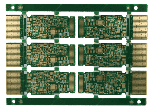
What Devices Actually Use Optical Module PCBs
Optical module PCBs sit inside pluggable transceivers, so the application list is really a list of where those transceivers plug in. What determines the right board tier is less the device category and more the data rate and physical space it has to fit into.
SFP+ transceivers in enterprise switches: Running at 10G or 25G, these modules tolerate standard high-Tg FR4 and a simpler 4 to 6 layer stackup, since signal margins are relatively forgiving at this rate.
QSFP28 modules in data center leaf-spine networks: At 100G aggregate, these need controlled differential impedance and a lower-loss laminate than SFP+ boards.
QSFP-DD and OSFP modules in AI cluster interconnects: Supporting 400G and 800G, these push into ultra-low-loss material territory with tight line width tolerance, because the space for signal margin shrinks as lane count and switching speed rise.
5G fronthaul radio units: Optical modules here face outdoor temperature swings, so material CTE match and surface finish durability matter as much as raw speed.
Active optical cables in high-performance computing: These embed the PCB directly at the cable end, so board thickness and gold finger chamfer tolerance become mechanical fit issues, not just electrical ones.
The device tells you the data rate; the data rate tells you the material and stackup tier the board actually needs.
Which Materials an Optical Module PCB Actually Needs
The core question a material choice answers is how much signal strength the board can afford to lose over its trace length at the target data rate. Laminates are generally grouped into loss tiers, and picking one below the tier your data rate needs is the single most common design mistake.
| Speed Tier | Typical Application | Dk Range | Df Range |
|---|---|---|---|
| Mid-loss | 10G / 25G SFP+ | 3.8 – 4.4 | 0.007 – 0.011 |
| Low-loss | 25G – 40G links | 3.6 – 3.9 | 0.007 – 0.009 |
| Very-low-loss | 100G QSFP28 | 3.4 – 3.7 | 0.004 – 0.005 |
| Ultra-low-loss | 400G / 800G QSFP-DD, OSFP | 3.0 – 3.4 | 0.002 – 0.0028 |
Insertion loss is the metric that ties material choice back to a pass or fail result: at 25 Gbps and above, industry practice generally targets under roughly 0.5 dB per inch of trace at the relevant frequency, a threshold defined more by the IEEE 802.3 Ethernet PHY specifications the link has to meet than by any single material's datasheet. A board built on a mid-loss laminate can meet a 10G budget comfortably and blow through a 100G budget on the same trace length. Matching laminate tier to data rate, not to what is cheapest per panel, is what keeps a design out of the very-low-loss and ultra-low-loss retrofit cycle later.
What Actually Drives the Design Decisions on an Optical Module PCB
Once the material tier is set, a handful of physical design choices determine whether the board performs at that tier in practice rather than just on paper.
Gold finger clearance and plating: The edge connector needs a defined keep-out from plated through-holes and the board outline, hard gold plating for repeated insertion cycles, and a specific bevel angle so the finger seats cleanly in the cage. Get any of these wrong and the module either won't seat or wears out early.
Long and short finger sequencing: Power pins are typically drawn longer than data pins so power stabilizes before data starts flowing, and disconnects last. Skipping this timing logic risks damaging the module's logic chips on hot removal.
Differential pair impedance control: At 25 Gbps per lane and above, differential impedance is commonly held to 85 or 100 ohms with a tolerance tighter than the ±10% acceptable on general-purpose boards, since any mismatch reflects signal back down the line.
Via structure and backdrilling: Unused via stubs on high-speed lines act like small antennas at gigahertz frequencies. Backdrilling removes the stub; blind, buried, and laser-drilled microvias keep routing density high in a board that has almost no room to spare.
Thermal path from the laser diode: TOSA and ROSA components generate concentrated heat in a footprint with no room for a fan. Thermal vias placed directly under the hot components, sometimes paired with a copper coin or buried copper block, carry that heat into the board and out to the module shell.
Get the material tier right and skip any one of these, and the board still won't hold up under sustained data traffic.
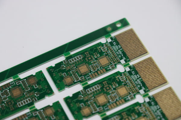
How PCBgogo Supports Optical Module PCB Gold Finger and Via Requirements
The gold finger and via requirements above are exactly where fabrication tolerance, not layout intent, decides whether a design actually works. PCBgogo's gold finger design rules call for at least 1.0mm clearance between the gold fingers and the board outline, no plated through-holes within 1.0mm of the fingers, a minimum board thickness of 1.0mm, and 30-degree edge beveling, the tolerances that keep an edge connector seating correctly in its cage.
On the via side, PCBgogo supports blind, buried, and via-in-pad structures along with laser-drilled microvias down to 3 to 6 mils, which cover the backdrilling and stub-control needs described above without forcing a redesign around what the fabricator can actually hold. Boards go up to 40 layers on Shengyi and Kingboard laminates, including high-Tg FR4 grades such as S1000-2, S1000-2M, and IT180A, a good fit for the mid-loss through very-low-loss tiers that cover SFP+ through QSFP28 designs. Every order gets AOI and X-ray inspection along with per-order DFM and engineer review before it runs, which is where gold finger clearance violations and via stub issues get caught before fabrication rather than after. For projects at the ultra-low-loss end of the table above, it's worth confirming laminate availability directly through PCBgogo's quoting tool before committing to a stackup.
Summary
An optical module PCB only performs as well as its weakest link among gold finger tolerance, laminate loss budget, and thermal path, and none of those three can compensate for a failure in the other two. Matching the material tier to the actual data rate, then verifying gold finger clearances and thermal via placement against what the fabricator can actually hold, is what separates a board that passes bench testing from one that holds up in the field. If you're mapping a design against manufacturing tolerances before committing to a stackup, PCBgogo's quoting tool gives a direct read on what's achievable for your layer count and material combination.
Frequently Asked Questions
What is an optical module PCB?
It is the internal circuit board inside a pluggable transceiver, such as an SFP, QSFP, or OSFP module, that carries the driver, receiver, and control circuitry converting electrical signals to optical signals and back.
Why do optical module PCBs use long and short gold fingers instead of equal-length ones?
The staggered lengths sequence power and data connection timing during hot insertion, so power stabilizes before data starts flowing and disconnects only after data stops, protecting the module's logic chips.
What PCB material is best for a 400G optical module?
A 400G design generally needs an ultra-low-loss laminate with Df in the roughly 0.002 to 0.003 range, since standard FR4 and even low-loss materials introduce too much signal attenuation at that lane rate.
How is heat managed on a PCB with almost no room to spare?
Thermal vias placed directly beneath the laser driver and TOSA/ROSA components, sometimes combined with a buried copper block or copper coin, conduct heat into the board and out to the module shell since fan-based cooling isn't an option inside the enclosure.
What impedance tolerance do these boards need?
At 25 Gbps per lane and above, differential impedance tolerance is commonly held tighter than the ±10% used on general-purpose boards, often in the ±5% to ±7% range, to limit signal reflection.
Can optical module PCBs use rigid-flex construction?
Yes, rigid-flex is increasingly used in compact form factors like QSFP-DD to fold circuitry into a tighter enclosure without adding connectors between sections.





