




 日本語
日本語
 한국어
한국어

What Are Mechanical Keyboard PCBs? A Practical Guide
KEY DEFINITION
A mechanical keyboard PCB is the circuit board that connects every switch, diode, controller, USB interface, and optional lighting feature. It converts key presses into digital input through a scanned row and column matrix, while its footprints and geometry determine which switches, layouts, plates, and cases will fit.
Key Takeaways
Lock the layout, switch standard, mounting method, and firmware before routing.
Use one correctly oriented diode per key for reliable multi-key input.
Treat the PCB, plate, stabilizers, case, and USB opening as one system with a shared origin.
For hot-swap designs, validate socket footprints, underside clearance, pad strength, and switch insertion loads.
Release fabrication, assembly, firmware, and test files together so the factory can verify finished behavior.
Introduction
A keyboard can look correct in CAD and still fail at assembly because one stabilizer opening, USB cutout, or hot-swap socket is misplaced. The mechanical keyboard PCB sits at the center of those dependencies, so early electrical and mechanical decisions directly affect typing feel, serviceability, firmware, and production yield.
This guide explains how the board works, how common PCB layouts differ, which components deserve the most attention, and how to prepare a design for dependable manufacturing.
What Is a Mechanical Keyboard PCB
A mechanical keyboard PCB is a rigid or flexible printed circuit board that senses switch closures and sends the corresponding key events to a computer or other host. Each switch connects a row to a column, and the microcontroller scans those lines repeatedly to identify the matrix position that changed.
The matrix reduces pin demand. A 5-row by 15-column matrix can represent 75 switch positions with 20 row and column signals instead of 75 individual microcontroller inputs. A diode placed in series with each switch controls current direction and prevents unintended paths when several keys are held, which is the electrical basis for reliable multi-key detection.
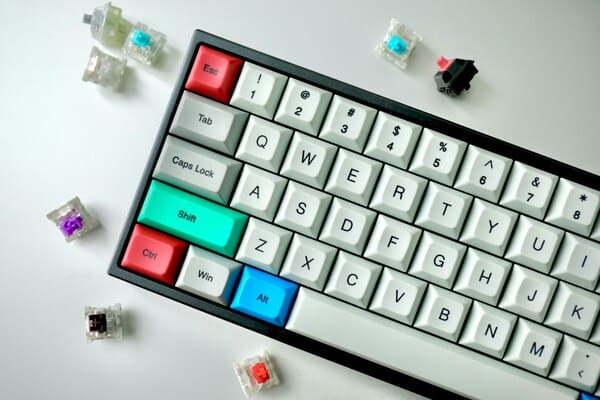
The board also fixes the physical geometry of the keyboard. A common MX-style grid uses 19.05 mm key spacing, but the PCB must still account for larger key units, stabilizers, stepped or split keys, encoders, displays, and alternative bottom rows. A PCB advertised for a given percentage size is therefore not automatically compatible with every case or plate in that category.
Once the PCB is understood as both a circuit and a mechanical reference, the next task is to define the design rules that keep those two roles aligned.
Mechanical Keyboard PCB Design Principles
Mechanical keyboard PCB design begins with a locked product definition: physical key positions, switch technology, plate and case geometry, firmware platform, connection method, and lighting behavior. Changing any of these after routing can affect footprints, controller pins, power demand, and board outline.
Matrix architecture: Assign rows and columns for clear routing. Keep every diode in the same direction, label matrix nets, and compare the schematic with firmware before release. Map each physical key to its matrix coordinate and firmware position.
Mechanical datum: Use one origin for the PCB outline, switch centers, plate, mounting holes, daughterboard, and case. Confirm stabilizer cutouts, then overlay the plate and PCB geometry. A label such as 65 percent is not a fit specification.
Hot-swap footprint control: Use the socket manufacturer's land pattern and confirm the socket side. Protect anchor pads, preserve the body keepout, and prevent screws, foam, batteries, or case ribs from occupying the same underside space.
Signal and power integrity: Route USB data as a close, matched pair with a 90 ohm differential target when controlled impedance is required. Put ESD protection near the connector and decoupling capacitors near controller power pins. Follow the radio module's antenna keepout on wireless boards.
RGB power budget: Calculate worst-case current before selecting the connector, regulator, traces, and firmware limit. An addressable RGB LED can approach 60 mA at full white, so 70 LEDs could request about 4.2 A. USB-powered products therefore need brightness limits and adequate bulk capacitance.
With these principles fixed, layout type becomes a deliberate product choice rather than a cosmetic label.
Mechanical Keyboard PCB Layout Types
Mechanical keyboard PCB layout types differ in key count, footprint density, navigation access, and mechanical compatibility. The values below are common planning references, but exact key counts and bottom row arrangements vary by design.
| Layout | Typical keys | PCB implication | Best fit |
|---|---|---|---|
| Full size | 104 or 105 | Largest outline, numpad included, more matrix positions | Office, data entry, users who need dedicated keys |
| Tenkeyless | 87 or 88 | Removes numpad while retaining function and navigation rows | General use with more mouse space |
| 75 percent | About 80 to 84 | Compact spacing increases routing and case coordination | Portable builds with a function row |
| 65 percent | About 66 to 68 | Dedicated arrows, fewer navigation keys, tight right edge | Compact daily use |
| 60 percent | About 61 | Minimal outline, functions move to firmware layers | Small cases and highly customized keymaps |
| Split or ergonomic | Varies | Two board halves, interconnect, mirrored geometry, added firmware setup | Ergonomic and adjustable positioning |
After choosing the layout family, freeze the exact keymap and mechanical drawing before selecting components, because component placement must fit around the switches rather than compete with them.
Key Components in Mechanical Keyboard PCB Manufacturing
The critical components are the parts that sense keys, process the matrix, communicate with the host, manage power, and survive assembly and daily use. Their footprints and placement should be reviewed together, not as isolated schematic symbols.
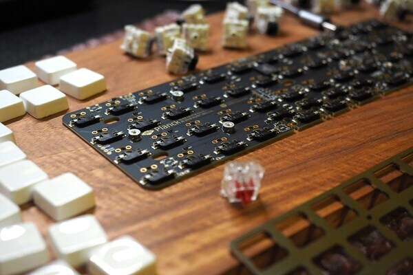
Switch footprints and sockets: Soldered MX style switches use plated through holes. Hot-swap versions add surface-mounted sockets, while low-profile and magnetic switches require different footprints and sometimes different sensing circuits. Never assume switch families are footprint compatible.
Diodes: One diode per key supports reliable simultaneous input. Its polarity mark should remain visible after placement and match the schematic convention.
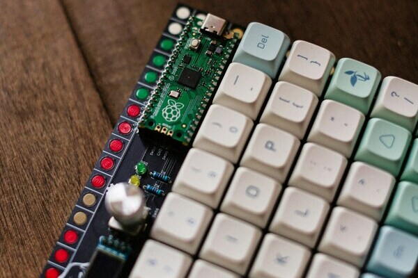
Microcontroller: The controller needs enough GPIO for the matrix and peripherals, plus memory for firmware and lighting. Integrated USB simplifies the interface, while a removable module makes prototypes easier to rework.
USB connector and protection: The Type-C footprint, shell tabs, board edge, and case opening must agree. Include the required configuration resistors, ESD protection, and anchoring for cable insertion.
Lighting and drivers: Backlighting, per-key RGB, and underglow have different routing and current needs. Coordinate reverse-mounted LEDs and light openings with the plate and case.
Optional controls: Encoders, displays, batteries, wireless modules, reset switches, and daughterboards consume pins and space. Keep service controls accessible and add programming and debug pads.
When the component set and placement are stable, the manufacturing package can be built around real inspection and functional test needs.
Mechanical Keyboard PCB Manufacturing Process
Mechanical keyboard PCB manufacturing turns the released electrical and mechanical data into tested bare boards and, when requested, fully assembled keyboard electronics. The most reliable workflow treats review, fabrication, assembly, programming, and validation as one controlled sequence.
Step 1. Design release and DFM review: Release fabrication and drill data, stackup, outline, impedance needs, assembly drawings, centroid data, BOM, and special instructions. Run electrical and design rule checks, then verify polarity, switch centers, and connector orientation.
Step 2. Bare PCB fabrication: The factory etches copper, drills and plates holes, applies solder mask and legend, adds the surface finish, routes the outline, and performs electrical testing. Two-layer FR4 at 1.6 mm with 1 oz copper is a common starting point. Dense RGB or wireless designs may benefit from four layers.
Step 3. Surface finish selection: ENIG is flat and supports fine surface-mount assembly. Lead-free HASL can be economical for conventional through-hole work but is less planar. Select the finish for assembly and storage needs, not sound claims.
Step 4. PCB assembly: Solder paste is printed, surface-mount parts are placed, and the board passes through reflow. Through-hole parts are soldered afterward. On hot-swap boards, inspect socket anchor joints because switch changes load those pads.
Step 5. Programming and functional test: Bare-board testing finds opens and shorts but cannot prove that every key reports correctly. Activate each matrix position, verify USB enumeration, and check LEDs and encoders. Provide firmware, the flashing method, device identity, and pass criteria.
Step 6. Pilot build and controlled scale-up: Assemble a pilot in the intended case with the actual plate, foam, stabilizers, switches, and cable. Convert recurring rework into drawing notes, footprint changes, or stronger test coverage before volume production.
This complete test path is also the basis for choosing a manufacturing partner that can support both the first prototype and repeat production.
Why PCBgogo Is the Best PCB Manufacturing Partner for Your Mechanical Keyboard Project
The best manufacturing partner for a mechanical keyboard project is one that can control the bare board, assembly, inspection, and test handoffs that most often create avoidable delays. PCBgogo brings those functions into a coordinated service that fits both validation builds and production releases.
One coordinated production path: PCBgogo supports bare PCB fabrication, component sourcing, SMT, through-hole, and mixed assembly. One partner reduces handoffs and helps trace whether a problem comes from the design, board, component, or assembly process.
Prototype-to-production flexibility: Assembly can start from one piece for matrix and case fit validation, then scale after the design and test fixture are stable.
Inspection matched to keyboard risks: Solder paste inspection and automated optical inspection target placement, polarity, and soldering defects. X-ray supports hidden joints, while flying probe, fixture testing, and customer-defined functional testing cover electrical and finished behavior.
Flexible sourcing models: Turnkey, partial turnkey, and consigned options let the customer control who purchases controllers, sockets, LEDs, connectors, and specialty parts.
Documented quality systems: PCBgogo lists ISO 9001, ISO 14001, ISO 45001, ISO 13485, IATF 16949, UL certification, and material compliance support. These systems support incoming inspection, traceability, and repeatable production records.
To get the most value from these capabilities, send a complete, revision-controlled package and define the functional test method before quoting. PCBgogo can then review the board against the actual assembly and acceptance requirements instead of relying on generic keyboard assumptions.
PCBgogo - Reliable, High-Quality PCB Manufacturing
Save time and money with an all-in-one solution for PCB fabrication, assembly, and parts. Reduce vendor coordination, avoid split shipments, and get consistent, reliable quality.
Get Free Quote >
Conclusion
A successful mechanical keyboard PCB combines a correct switch matrix with precise mechanical geometry, controlled power and USB design, manufacturable footprints, and a test plan that checks every real function. Freeze the layout early, validate a complete pilot in the final case, and give PCBgogo the fabrication, assembly, firmware, and test data needed to produce a repeatable result.
Frequently Asked Questions
Can a mechanical keyboard PCB fit any case of the same size?
No. Size labels do not define mounting holes, USB location, outline, plate geometry, or bottom row. Compare dimensioned drawings or 3D models before ordering.
Is a hot-swap PCB better than a soldered PCB?
Hot-swap suits frequent switch changes and field replacement. Soldered PCBs often support more layout options and need no underside socket clearance, so choose by serviceability and layout.
How many PCB layers does a mechanical keyboard need?
Two layers can handle many wired keyboards with straightforward matrix and USB routing. Four layers can simplify return paths, power distribution, dense RGB, wireless integration, and electromagnetic control.
Why does each key need a diode?
A diode prevents unintended current paths when multiple keys are pressed. Without suitable isolation, the controller can report a key that was not pressed or miss certain combinations.
What files should be sent for mechanical keyboard PCB assembly?
Send fabrication and drill data, stackup, outline, BOM, centroid data, assembly drawings, firmware, and test instructions. Include plate and case drawings when connector or mounting alignment is critical.
How should a mechanical keyboard PCB be tested before mass production?
Check the schematic and layout, then test bare-board continuity and shorts. After assembly, flash production firmware and verify every switch, LED, encoder, connector, and wireless function in the final mechanical stack.





