
Lead Solder vs. Lead-Free Solder: Which One Does Your PCB Actually Need?
Walk into any electronics workshop and you'll find both lead solder and lead-free solder on the shelf. Engineers argue about them. Procurement teams ask about compliance. Hobbyists just want to know which one works better. The short answer is: it depends on what you're building, where it's going, and what tradeoffs you can live with.
This guide breaks down the real differences — from melting points and joint reliability to regulatory requirements and surface finish compatibility — so you can make an informed decision before your boards go into production.
What Is Lead Solder?
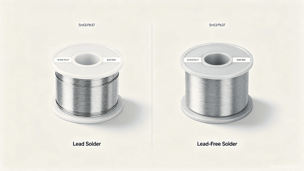
Lead solder — also called leaded solder — is a metal alloy traditionally made from tin and lead. The most common formulation is Sn63/Pb37, which is 63% tin and 37% lead. This particular ratio is eutectic, meaning it melts and solidifies at a single temperature (183°C / 361°F) rather than passing through a mushy phase.
That predictable phase transition is a big deal in electronics assembly. It reduces the risk of disturbing a joint while it's solidifying, which is one of the main causes of cold solder joints. Combined with its low melting point, excellent wettability, and self-fluxing properties, leaded solder became the industry standard for decades.
Other common formulations include Sn60/Pb40 (slightly higher melting range, 183–190°C) and Sn10/Pb90, used in high-temperature applications like wave soldering pallets.
What Is Lead-Free Solder?
Lead-free solder replaces lead with other metals. The most widely used alloy today is SAC305 — 96.5% tin, 3% silver, 0.5% copper — with a melting point of around 217–220°C. Other variants include SAC405 (higher silver content) and low-silver alternatives like SN100C (tin-copper-nickel) favored for wave soldering applications.
The push toward lead-free assembly was largely driven by the EU's RoHS (Restriction of Hazardous Substances) Directive, which took effect in 2006 and limited the use of lead in most consumer electronics. Today, lead-free is the default for anything sold in the EU, and most manufacturers have adopted it globally to simplify supply chains.
Lead vs. Lead-Free Solder: Side-by-Side Comparison
| Property | Lead Solder (Sn63/Pb37) | Lead-Free (SAC305) |
|---|---|---|
| Melting Point | 183°C (361°F) | 217–220°C (422–428°F) |
| Wettability | Excellent | Good (requires active flux) |
| Joint Reliability | Very high (eutectic) | High (alloy-dependent) |
| Tin Whisker Risk | Very low | Higher without mitigation |
| RoHS Compliance | No (exemptions apply) | Yes |
| Process Temperature | Lower (less thermal stress) | Higher (~30–40°C more) |
| Cost | Lower | Higher (silver content) |
Performance and Reliability: Where Each Excels
For most consumer electronics, lead-free solder performs comparably to leaded — especially with modern SAC alloys and optimized reflow profiles. But there are specific scenarios where each type has a clear edge.
Lead solder tends to outperform in:
High-vibration environments — leaded joints are more ductile and absorb mechanical stress better
Rework-heavy assemblies — lower reflow temperatures reduce the risk of damaging nearby components
Fine-pitch and high-density boards — better wettability means cleaner joints in tight spaces
Military and aerospace applications — where RoHS exemptions allow leaded solder for its proven long-term reliability
Lead-free solder has the advantage when:
RoHS or REACH compliance is required for market access
Products may be exposed to high operating temperatures (lead-free joints hold up better above 150°C)
Environmental regulations in the target market prohibit lead content
End-of-life recycling and disposal requirements are a concern
Lead Solder Safety: Separating Fact from Fiction
A lot of the alarm around lead solder is real, but some of it is overstated. Lead is genuinely toxic — it accumulates in the body over time and poses serious health risks with prolonged or repeated exposure. The actual hazard in a soldering context, though, comes primarily from fumes (which are mostly flux vapors, not lead vapor) and from ingesting lead particles via unwashed hands.
Simply handling leaded solder wire with bare hands carries minimal risk as long as you wash up afterward. The more significant occupational exposure comes from years of daily soldering without proper ventilation or hygiene. In a controlled manufacturing environment with proper extraction systems, lead solder can be used safely.
Basic precautions include:
Always work with adequate ventilation or a fume extractor
Wash hands thoroughly before eating, drinking, or touching your face
Avoid sanding or grinding leaded solder joints, which generates fine particles
Store and dispose of leaded materials according to local regulations
Surface Finish Compatibility: Why It Matters
Solder selection doesn't happen in isolation — it directly interacts with your PCB's surface finish. This is especially important if you're working with hard gold plating on PCBs.
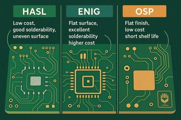
Hard gold plating (electroplated gold, typically over nickel) is commonly used on edge connectors, card contacts, and high-wear areas. It's extremely durable and corrosion-resistant, but it's not ideal as a solderable surface — gold dissolves rapidly into solder, which can cause gold embrittlement and weak joints, particularly with SAC alloys. For components that will be soldered, ENIG (Electroless Nickel Immersion Gold) is a better choice: it provides a thin, uniform gold layer over nickel that protects solderability without the embrittlement risk.
When specifying hard gold plating on a PCB, it's typically used on connector areas only, with a different finish (HASL, ENIG, or OSP) on the solderable pads. Getting this distinction right during design — and flagging it clearly in your fabrication notes — prevents a lot of assembly headaches downstream.
So Which Should You Use?
Here's a simple way to frame it:
Choose lead solder if:
Your product is exempt from RoHS (military, aerospace, medical under certain conditions)
You're doing prototype work or rework where process control is harder to maintain
The application involves high vibration or mechanical shock
You're working with legacy components rated for leaded processes
Choose lead-free solder if:
You're shipping to the EU, UK, California, or any market with RoHS/REACH requirements
Your product is consumer electronics or IoT
Long-term environmental disposal is a concern
Your component library is sourced from RoHS-compliant suppliers
Final Thoughts
Your solder choice directly influences how a PCB should be designed and manufactured. Differences in reflow temperature can affect material selection, stack-up stability, component placement accuracy, and solder mask performance — which is why getting the process aligned early helps avoid issues like delamination or poor solder wetting later in production.
At PCBgogo, we use mature manufacturing processes and high-quality materials to ensure stable performance across different assembly requirements. If you're not sure which surface finish or production approach best fits your project, feel free to get in touch — our engineering team will review your design and recommend a practical, reliable solution to help you move forward with confidence.


