



 日本語
日本語
 한국어
한국어

Design Power Bank Module at Home A Practical PCB Guide
KEY TAKEAWAYS1. Use a complete power architecture: Include charging, protection, load sharing, 5 V conversion, current limiting, and thermal control.2. Treat the battery as safety-critical: Use a new, documented cell and never solder directly to an untagged cylindrical cell.3. Prototype in stages: Verify the charger, boost stage, protection, and load switching before a full power test.4. Design around current flow: Keep loops short, ground solid, and ceramic capacitors close to the IC pins.5. Plan production data early: Gerbers, BOM, centroid data, drawings, and test limits turn one working board into a repeatable build.
A power bank looks simple from the outside, yet its PCB must manage a cell whose voltage changes from roughly 3.0 V to 4.2 V while presenting a stable 5 V output. A weak layout can pass a no-load test and still reset, overheat, or oscillate when a phone draws current.
This guide explains how to design a power bank module at home as an engineering project, including the circuit blocks, parts list, assembly precautions, validation steps, applications, and the path from a bench prototype to controlled PCB production.
How a Power Bank Module Works
A power bank module charges one lithium-ion cell with a constant current and constant voltage profile, then boosts the cell voltage to a regulated 5 V output when a load is connected. The protection path disconnects the cell during overcharge, deep discharge, short circuit, or excessive current, while a power path controller prevents the input supply and battery from fighting each other.
For a basic 5 V USB-C input, each CC pin needs its own 5.1 kOhm pull-down resistor to identify a sink. USB Power Delivery needs a dedicated controller and firmware. A USB-C output also requires correct Type-C source control.
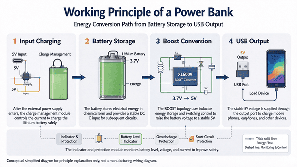
The drawing is functional, not a drop-in circuit. Use the exact device datasheets for reference values, compensation, inductor range, and placement because pin-compatible parts may need different support components.
Power Bank Module Component List
The component list for a practical module must cover energy storage, conversion, connection, protection, and test access. The table gives engineering selection criteria rather than locking the design to one vendor or an obsolete part number.
| Part | Typical requirement | Qty | Selection note |
|---|---|---|---|
| 1S lithium-ion cell | 3.6 or 3.7 V nominal | 1 | Use a new protected cell or add a protection circuit. Confirm capacity and discharge rating. |
| Charger with power path | 4.2 V for standard cell | 1 | Requires current control, load sharing, thermal regulation, and NTC support. |
| Boost converter | 5 V regulated output | 1 | Choose synchronous conversion and a suitable current limit. |
| Protection IC and MOSFETs | 1S overvoltage and undervoltage | 1 set | Required when protection is not integrated into the cell or power management IC. |
| Inductor | Datasheet value | 1 | Check saturation current, DC resistance, and temperature rise. |
| Ceramic capacitors | X7R preferred | 6 to 10 | Allow for DC bias derating and place them at the IC pins. |
| USB connectors and ESD | Ports as designed | 2 sets | Use reinforced shells and protect exposed pins. |
| Resistors, NTC, fuse | 1 percent and rated parts | as needed | Set currents, sense temperature, and limit fault energy. |
| PCB and test points | FR 4 with adequate copper | 1 | Expose battery, input, output, ground, enable, and current nodes. |
Power Bank Module Assembly Precautions
Safe assembly depends on controlling cell energy, polarity, soldering heat, and the first power-up sequence. Before you design a power bank module at home, set up a nonflammable work surface, eye protection, a current-limited bench supply, and a way to isolate the cell quickly.
Cell condition: Reject swollen, dented, salvaged, or undocumented cells. Never mix different cell types or ages.
Connection method: Use a holder, welded tabs, or a prepared pack. Direct soldering can damage the cell.
Polarity control: Mark battery, input, output, and ground. Add reverse protection for a replaceable cell.
Thermal control: Put the NTC on the cell away from the inductor. Stop if any part heats rapidly.
First power up: Substitute a 3.7 V current-limited supply and confirm quiescent current before connecting the cell.
Battery chemistry and maximum charge voltage must match the charger. Standard 4.2 V lithium-ion, 4.35 V high voltage, and 3.2 V lithium iron phosphate cells are not interchangeable.
How to Build a Power Bank Module Step by Step
The most reliable home build separates specification, circuit validation, assembly, and load testing into controlled steps. This sequence catches wrong assumptions before the battery supplies enough fault current to damage the board.
Step 1: Define the electrical target. Choose the cell, 5 V input, output current, runtime, connectors, and enclosure. A 5 V 1 A target is easier to validate than 5 V 3 A.
Step 2: Estimate the real battery current. At 5 V and 1 A, the load consumes 5 W. With 90 percent conversion efficiency and a 3.7 V cell, the approximate cell current is 5 divided by 0.90 divided by 3.7, or 1.50 A. Size the cell, MOSFETs, inductor, connector, and copper for this input current plus margin.
Step 3: Select the architecture. Use power path control when the load must run during charging. Pair it with a synchronous boost converter or a suitable integrated controller.
Step 4: Capture the schematic. Add ESD, USB-C CC resistors, charger parts, protection, NTC, boost parts, current limiting, shields, and test points. Run electrical rule checks.
Step 5: Prototype without the cell. Drive the battery rail from a current-limited supply. At 3.0 V, 3.7 V, and 4.2 V, verify output, no-load current, and current limit with an electronic load.
Step 6: Assemble and inspect. Solder small parts first, inspect polarity and bridges, then measure resistance from the battery and 5 V rails to ground before connecting a cell.
Step 7: Test charging. Connect the correct cell through a protected lead. Record charge current, battery voltage, input current, and temperature, then confirm termination.
Step 8: Test output transitions. Sweep from zero to rated load, record voltage and temperature, and plug or unplug input power under load. Check for resets and backfeed.
Step 9: Check faults cautiously. With a protected fixture, verify output short recovery, low battery shutdown, and connector heating. Never short or puncture the cell.
Step 10: Freeze the build. Save the schematic revision, firmware, exact BOM, measurements, and approved substitutions as the PCB prototype baseline.
Power Bank Module Applications
A power bank module is useful wherever a 1S rechargeable battery must provide a controlled 5 V rail, but the correct output rating and interface depend on the actual load.
Portable sensor node: It can run data loggers and field sensors. Low quiescent current matters during long sleep periods.
Router backup supply: Confirm voltage, startup surge, and runtime first. Many routers need 9 V or 12 V rather than 5 V.
Microcontroller prototype: It can power development boards, but switching current must stay away from analog sensor grounds.
LED task light: A USB light still needs correct LED current control and thermal management.
Emergency phone charging: Basic 5 V charging is practical. Fast charging requires protocol control and more thermal margin.
These use cases also reveal why the prototype should be converted into a PCB only after the target load and fault behavior are measured.
From a Home Build to a PCB Prototype and Production
Moving from a home build to production means turning a functioning circuit into controlled manufacturing data and objective acceptance tests. A solderless board is useful for logic, but switch-mode power stages need a PCB because trace inductance, ground return geometry, and thermal spreading directly affect performance.
Lay Out the Power Stage for Current and Heat
Place the boost input capacitor, switching IC, inductor, synchronous switching path, and output capacitor as a tight cluster. Keep the switching node small and away from the NTC, CC pins, feedback divider, and USB data lines. Use uninterrupted ground under control circuitry, multiple thermal vias under exposed pads when the datasheet calls for them, and wide copper or pours for the cell and 5 V paths.
Choose copper width from current, temperature rise, copper thickness, and stackup. Review connector current density and board edge reinforcement as carefully as the converter.
Create a Complete Prototype Package
Release fabrication data, drill files, stackup, BOM, centroid data, assembly drawing, polarity notes, and test limits. Add accessible points for input, cell, output, ground, enable, and NTC signals.
Test every pilot board for shorts, standby current, charging, regulation, load, shutdown, and connector integrity. Measure temperature at rated load inside the intended enclosure.
Scale the Verified Design with PCBgogo
Once files and limits are stable, quality depends on controlled fabrication, parts, assembly, and inspection. PCBgogo supports PCB fabrication, sourcing, SMT and through-hole assembly, inspection, and testing from prototypes through volume production.
Quality control: Specify IPC class, substitutions, polarity, and test criteria. PCBgogo offers visual inspection and AOI capability, with X-ray for BGA assemblies.
Advanced processes: Available assembly options include rigid FR 4, flexible, rigid flex, and metal core boards. Select construction based on measured current and heat.
Delivery planning: Schedules depend on parts and inspection. Coordinated fabrication and assembly reduce handoffs and support a confirmed production plan.
Engineering service: Provide the schematic, fabrication data, BOM, centroid file, drawings, and test instructions for review before production.
One-stop transition: A single workflow helps preserve the approved stackup, parts, revision, and acceptance standard as volume increases.
Before batch release, approve the golden sample, freeze the revision, define serialized or lot-based traceability if needed, and require formal approval for substitutions. That process provides more confidence than judging quality from a single working sample.
PCBgogo - Reliable, High-Quality PCB Manufacturing
Save time and money with an all-in-one solution for PCB fabrication, assembly, and parts. Reduce vendor coordination, avoid split shipments, and get consistent, reliable quality.
Get Free Quote >
Conclusion
To design a power bank module at home successfully, treat charging, protection, conversion, thermal behavior, and PCB current flow as one system. Validate each block with current-limited equipment, document the measured limits, and move to PCB production only after the prototype passes load, transition, and temperature tests. When the design package is ready, PCBgogo can support the controlled move from prototype boards to assembled production batches.
Frequently Asked Questions
Can I build a power bank module without a protection circuit
No. Lithium-ion designs need verified protection against overcharge, deep discharge, overcurrent, and short circuit, whether in the pack, controller, or a separate IC.
Can I charge a phone directly from a 3.7 V lithium-ion cell
No. Basic phone charging expects regulated 5 V. A varying cell voltage needs a boost converter and correct port control.
Why does the 5 V output drop when I connect a load
Check the cell, inductor saturation, current limit, resistance, capacitor placement, and DC bias derating. Measure cell voltage and input current with an electronic load.
Can a power bank charge and power a load at the same time
Yes, with power path control and adequate thermal margin. A simple parallel load can disrupt charge termination.
Do I need a four-layer PCB for a power bank module
Not always. Two layers can support modest power, while four layers may improve ground and heat spreading. Base the choice on current, size, EMC, and thermal tests.





