



 日本語
日本語
 한국어
한국어

Custom Keyboard PCB Turnkey Service: Design, Prototype to Mass Production
KEY TAKEAWAYS1. Freeze the switch layout, plate geometry, stabilizer positions, and case mounting points before routing the PCB.2. Choose soldered or hot-swap switches early; the socket footprint, retention strategy, assembly cost, and service plan differ.3. Use a prototype to verify every key, USB connection, lighting circuit, and mechanical fit before approving a production panel.4. Send one controlled release package with fabrication files, BOM, placement data, drawings, firmware, and test requirements.
A custom PCB keyboard project can look electrically simple until the first assembled board meets the plate and case. A switch that misses its cutout by a fraction, a reversed hot-swap socket, or a USB connector without support can turn a good schematic into an expensive revision.
This guide follows the board from layout choices through prototype validation and repeatable production, so designers and purchasing teams can brief a turnkey supplier with fewer assumptions.
What Is a Keyboard PCB?
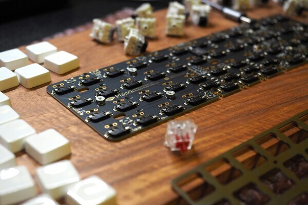
A keyboard PCB is the circuit board that connects switch inputs to a controller and carries power, data, and optional lighting. Most mechanical designs scan a row and column matrix: firmware drives one set of lines and reads the other to identify pressed keys. A diode at each switch position controls current direction and prevents ghosting when several keys are held together.
The PCB also fixes the physical relationships among switches, stabilizers, mounting holes, connector, and case. It may carry a microcontroller directly or connect to a separate controller module. The bare PCB is only part of the deliverable; an assembled keyboard PCBA may also include sockets, diodes, LEDs, protection parts, and the USB connector.
Why Choose a Custom Keyboard PCB?
A custom PCB is justified when a standard board cannot meet the product's layout, enclosure, features, or supply plan. A compact split keyboard may need a nonstandard outline and interconnect. A commercial board may need a specific USB location, per-key lighting, or a controller that can be sourced throughout its production life.
Customization also lets the team set serviceability and cost targets. Hot-swap sockets simplify switch replacement but consume board area and add assembly steps. Soldered switches cost less in parts and can suit a fixed product configuration. Make this choice based on expected repair volume and user behavior, not only an initial prototype bill of materials.
Design Principles for a Custom Keyboard PCB
The best starting point is a mechanical drawing that defines key spacing, switch orientation, plate cutouts, stabilizer types, PCB outline, and mounting holes. Keep the PCB origin and revision consistent across CAD, fabrication, and assembly files. Before layout release, print a 1:1 outline or make a simple mechanical sample and compare it with the enclosure.
For the electrical design, assign each switch to a documented matrix position and verify that the controller has enough usable GPIO after USB, lighting, and other functions are reserved. Place each switch diode with a consistent polarity and label it clearly. If a design uses multiple physical layouts, confirm that alternate footprints do not create unintended copper connections or assembly ambiguity.
Keep USB D+ and D- as a short, well-referenced pair with the connector maker's footprint and recommended routing in mind. Add suitable ESD protection near the external port, provide a stable ground return, and avoid placing a mounting screw or metal case feature where it can short exposed pads. Check the connector's insertion force and enclosure support; solder joints should not be the only structure resisting repeated cable use.
A useful prototype test plan is concrete: check continuity and shorts, flash firmware, press every switch position, test simultaneous key combinations, exercise every LED, and plug and unplug USB repeatedly while watching for intermittent connections. Record failures against the PCB revision so fixes carry into production rather than disappearing in informal notes.
Key Components in Keyboard PCB Manufacturing
The component choices determine the board footprint, assembly method, and inspection points. Lock the exact manufacturer part number before releasing the production BOM.
1. Switches
Specify the switch family and footprint, pin count, orientation, and whether the plate or PCB provides mechanical support. An MX-compatible footprint does not automatically accept every low-profile or optical switch. Verify pin locations, body clearance, and stabilizer interference with the selected switch datasheet and a physical sample.
2. Stabilizers
Stabilizers support wide keys such as Space, Enter, and Shift. PCB-mounted and plate-mounted versions need different keepouts and holes. Place the chosen stabilizer footprint from the actual keycap unit size, then check screw heads and clips against traces on both sides of the board.
3. Hot Swap Sockets
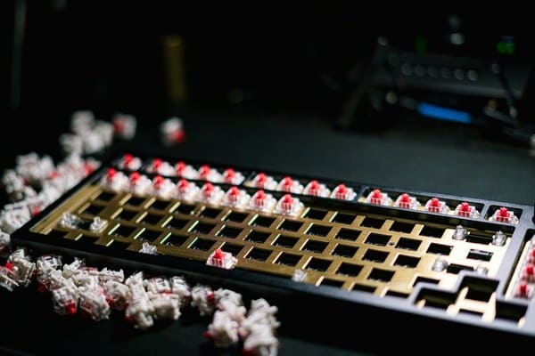
Hot swap sockets let users replace compatible switches without desoldering. Their pads need the exact vendor footprint, correct side and rotation, and enough surrounding clearance for assembly and rework. Frequent switch changes load the socket mechanically, so confirm plate support and test insertion before ordering a large batch.
4. LEDs
Single-color backlights and addressable RGB LEDs use different circuits and firmware resources. Check LED height against switch and plate geometry, diffuser clearance, power budget, and data direction. For RGB, prototype the worst-case brightness so the USB power path and thermal behavior are understood before the lighting feature is advertised.
5. Controllers
Choose a controller for available GPIO, USB support, memory, firmware ecosystem, and long-term sourcing. Reserve programming and recovery access. A compact MCU package can reduce board area, but it increases assembly and rework difficulty, so choose the package with the expected production volume in mind.
6. Interface Connectors
USB-C receptacles, daughterboard connectors, and split keyboard interconnects require matching pinouts and mechanical retention. For a USB-C device port, provide the required configuration channel resistors and check the exact connector footprint. Define cable orientation and external mating parts in the build package to prevent a board that passes electrical test but does not fit the case.
Material Choices for a Custom Keyboard PCB
Most keyboard PCBs are rigid FR-4. A common 1.6 mm thickness offers familiar switch and case geometry, but the correct thickness is whatever the socket, switch, plate, and enclosure stack up require. A thinner board may flex more in a gasket design; a thicker board changes connector and mounting fit. Ask the fabricator to confirm available thickness tolerance before locking the case tooling.
Two copper layers usually cover a wired keyboard matrix and modest lighting. Four layers can simplify ground continuity and dense routing on a compact, wireless, or RGB-heavy design, but add cost. Choose copper weight from current and trace geometry rather than treating heavier copper as a default quality upgrade. For surface finish, ENIG provides a flat solderable surface useful for fine pitch parts and exposed pads; evaluate its cost against the assembly need. Specify solder mask color for appearance only after confirming the finish and inspection plan.
Manufacturing Techniques: When and Why They Matter
The process should match the design risk. A conventional routed two-layer FR-4 board with standard drilled vias is often sufficient for a wired keyboard. The following techniques become valuable when the layout or release volume calls for them:
| Technique | Use it when | Why it matters |
|---|---|---|
| Panelization with tooling rails | Small or irregular boards enter automated assembly | Provides handling edges and repeatable placement; confirm breakaway tabs avoid visible or stressed areas. |
| Laser-cut stainless stencil and SMT reflow | Diodes, LEDs, controller, or hot swap sockets are SMT parts | Controls paste volume and makes assembly more consistent than hand soldering. |
| AOI and electrical test | Every production lot, especially dense LED and socket layouts | Finds polarity, placement, solder, open, and short defects before final keyboard testing. |
| X-ray inspection | Hidden joints such as BGA devices are selected | Checks joints that visual inspection cannot see; avoid BGA unless the design needs it. |
| Controlled depth routing or castellated edges | A module or enclosure specifically requires them | Supports special mechanical or interconnect geometry after a drawing-level review. |
Do not add advanced processes simply to make the specification look sophisticated. Define the stackup, minimum clearances, finish, and test method from real product requirements, then ask for a design for manufacturability review before releasing tooling. For production, use a golden sample and a functional test fixture that scans every matrix position, checks lighting, and verifies USB enumeration.
Why PCBgogo Is a Practical Manufacturing Partner
A custom keyboard PCB is more than a bare circuit board. It must fit the case and plate, match the selected switches and stabilizers, support stable firmware operation, and perform consistently across every production batch. PCBgogo brings PCB fabrication, component sourcing, assembly, inspection, and testing into one coordinated workflow, making it easier to move from the first prototype to mass production.
Quality control focused on real keyboard defects: A broken matrix trace, reversed diode, poorly soldered hot-swap socket, or misaligned USB connector can make an otherwise finished keyboard unusable. PCBgogo combines electrical testing with visual inspection and automated optical inspection. Flying probe testing is suitable for prototypes and small batches, while fixture-based testing can improve efficiency for repeat production. X-ray inspection is also available when the design includes components with hidden solder joints.
Manufacturing support for both simple and advanced designs: PCBgogo supports rigid FR-4, rigid-flex construction, SMT assembly, through-hole assembly, and mixed assembly. This allows the same manufacturing partner to handle anything from a straightforward two-layer wired keyboard to a compact board with per-key RGB lighting, fine-pitch controllers, daughterboards, or space-constrained routing.
Flexible sourcing and assembly options: Customers can choose full turnkey assembly, partial turnkey assembly, or consigned components. PCBgogo can source standard components such as diodes, resistors, capacitors, connectors, and controllers, while the customer supplies specialized parts such as switches or proprietary modules. This flexibility is especially useful when certain components have approved suppliers, limited availability, or strict branding requirements.
A smoother path from prototype to production: Early prototypes help verify the key matrix, USB connection, LED behavior, firmware programming, and mechanical fit before a larger order is released. Once the design is approved, the same manufacturing data can support pilot production and repeat orders, reducing the risk of errors caused by transferring files between multiple suppliers. Expedited fabrication and assembly options are available when the design files and components are ready.
For the best result, provide a complete and revision-controlled package that includes Gerber and drill files, the BOM, component placement data, assembly drawings, approved substitutions, firmware, and a functional test procedure. A tested golden sample can then serve as the acceptance reference for switch response, lighting, USB operation, connector alignment, and enclosure fit.
With coordinated fabrication, sourcing, assembly, and inspection, PCBgogo helps turn a custom keyboard design into a production-ready PCBA while giving engineering teams clearer control over quality, lead time, and repeatability.
PCBgogo - Reliable, High-Quality PCB Manufacturing
Save time and money with an all-in-one solution for PCB fabrication, assembly, and parts. Reduce vendor coordination, avoid split shipments, and get consistent, reliable quality.
Get Free Quote >
Conclusion
A successful custom PCB keyboard starts with mechanical fit and a complete electrical specification, then proves both in a tested prototype. Choose materials and manufacturing processes to solve specific layout and volume needs, and carry one controlled release package into the pilot and production builds. PCBgogo can support the fabrication, sourcing, assembly, and inspection stages when the build requirements and functional acceptance tests are clearly defined.
FAQ
Can I use one PCB for both soldered and hot swap switches?
Sometimes, but only if the footprints, routing, and mechanical clearances are deliberately designed for both. Check socket orientation and switch pin access in a prototype; do not assume an overlapping footprint is manufacturable.
Is a two-layer PCB enough for a custom keyboard?
Usually for a wired matrix with modest lighting. Dense RGB, wireless circuitry, or tight form factors may benefit from four layers for cleaner power and ground routing.
What files are needed for a turnkey keyboard PCBA quote?
Provide fabrication files, drill data, outline and stackup notes, BOM with manufacturer part numbers, placement data, and assembly drawings. Add firmware, a programmed test image, and pass or fail criteria if the supplier will perform functional testing.
How should I validate a prototype before mass production?
Build it in the intended plate and case, then test every key, multi-key combinations, lighting, USB connection, and firmware recovery. Keep a signed golden sample and a revision-specific test record for the pilot lot.





