
 日本語
日本語
 한국어
한국어

Amplifier PCB: The Complete Guide to Design, Components, and Layout
An amplifier PCB is the physical circuit board that takes a weak electrical signal and boosts it into something strong enough to drive a speaker, an antenna, a motor, or another downstream circuit. Every audio system, RF transmitter, sensor front-end, and power supply relies on one, which is why getting the layout right has such an outsized effect on how the finished product sounds, performs, and survives in the field.
This guide walks through what an amplifier PCB actually is, the components that make it work, the different types you'll encounter, and the layout practices that separate a clean, stable design from one that hums, oscillates, or overheats.
What Is an Amplifier PCB?
At its core, a pcb board amplifier arranges transistors, op-amps, resistors, capacitors, and inductors into a circuit that increases the amplitude of an input signal without distorting it. The board typically breaks down into three functional zones:
Input stage — receives the weak incoming signal and needs quiet, low-noise routing since any interference picked up here gets amplified along with the signal.
Gain/output stage — where transistors or an amplifier IC do the actual work of boosting current or voltage to drive the load.
Power and grounding network — supplies clean energy to the active devices and gives return currents a well-defined path back to source.
The job of the PCB designer is to connect these three zones so that gain is high and predictable, noise stays low, and heat has somewhere to go.
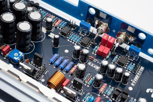
Key Components of an Amplifier PCB Circuit
Transistors and amplifier ICs. Bipolar junction transistors (BJTs) and MOSFETs form the backbone of most power stages — BJTs for linear gain, MOSFETs for efficient switching in Class-D designs. In signal-level circuits, an operational amplifier (op-amp) often replaces discrete transistors entirely, handling gain, filtering, and buffering in a single package.
Resistors. Beyond simply limiting current, resistors set the gain of feedback networks and bias the active devices into their correct operating point. Precision resistors in feedback loops matter more than people expect — a loose tolerance here shows up directly as gain error or instability.
Capacitors. Capacitors filter supply noise, block DC where it isn't wanted, and shape frequency response. Decoupling capacitors placed right at the power pins of an IC are one of the single most effective ways to keep an amplifier stable.
Inductors and EMI filters. These suppress high-frequency switching noise, which matters most in Class-D amplifiers and RF power stages where fast edges generate broadband interference.
Heat sinks and thermal vias. Any amplifier that handles real power dissipates heat as a byproduct. Copper pours, thermal vias, and physical heat sinks all work together to move that heat away from sensitive junctions.
Types of Amplifier PCBs
Amplifier PCBs aren't one-size-fits-all — the right approach depends heavily on the signal being amplified and the power involved.
Power amplifier PCBs step up the magnitude of a signal so it can drive a demanding load, such as taking a line-level audio signal and delivering enough current to move a speaker cone.
Audio amplifier PCBs are classified by amplifier class. Class A offers the cleanest signal but wastes the most energy as heat; Class B and AB trade a little linearity for much better efficiency; Class D switches at high frequency and wastes very little power, which is why it dominates modern compact audio gear.
RF and microwave power amplifier PCBs amplify signals meant to travel over the air across long distances. These designs live and die by controlled impedance, careful transmission-line geometry, and rigorous component selection, since even small layout mistakes cause reflections and signal loss at high frequencies.
Operational amplifier PCBs handle precision, low-power signal conditioning — think instrumentation amplifiers, sensor front-ends, and headphone-level circuits — where the priority is accuracy rather than raw power output.
How Layout Affects Performance
A schematic that works perfectly in simulation can still fail on a physical board if the layout ignores a few physical realities. Copper traces have resistance, inductance, and capacitance; every loop of current acts a little like an antenna; and every junction that gets hot enough will eventually drift or fail. Amplifier layout is really about managing these three effects — resistance, radiated noise, and heat — simultaneously.
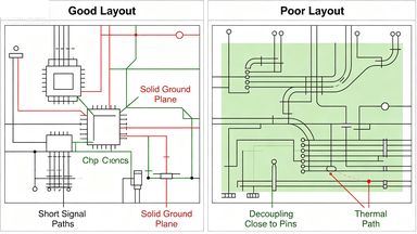
Keep Signal Paths Short and Direct
The smaller the loop formed by a signal trace and its return path, the less noise it picks up and the less it radiates. Feedback and input traces are the most sensitive part of an amplifier PCB circuit and should sit as close to the IC pins as the footprint allows, routed away from switching regulators or other noisy areas of the board.
Ground the Board Deliberately
Rather than letting ground connections happen wherever is convenient, effective designs use a star ground — a single point where analog, digital, and power grounds all converge — so return currents from noisy sections can't sneak back through a sensitive analog path and reintroduce hum. Solid ground and power planes, rather than thin traces, further cut impedance and give the whole board a more stable reference.
Route with Geometry in Mind
Sharp 90-degree corners create minor impedance discontinuities and etching artifacts, 45-degree bends or gentle curves route current more smoothly and reduce radiated emissions. High-current traces should be as wide as the board allows, and sensitive low-level signal lines should never run parallel to or cross over power traces.
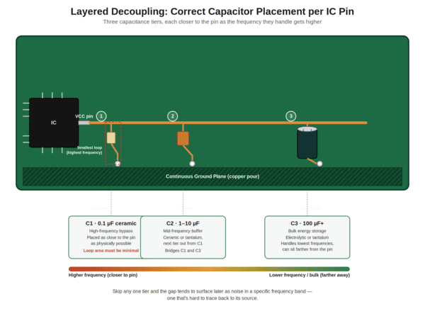
Decouple Every Active Device
A layered approach works best: a small ceramic capacitor (around 0.1 μF) for high-frequency noise placed as close to the pin as physically possible, a mid-value capacitor (1–10 μF) for the next tier of frequencies, and a larger electrolytic or tantalum capacitor (100 μF or more) to handle bulk energy storage. Skipping any one tier tends to show up later as noise at a specific frequency band that's hard to trace back to its source.
Manage Heat Before It Becomes a Problem
Heat should have a clear, low-resistance path away from the device generating it: from the chip, into a wide copper pad, through an array of thermal vias, and out to a ground plane, heat sink, or the opposite side of the board. Spreading heat this way can lower junction temperature substantially compared to a design with minimal copper around the hot components, which translates directly into longer component life and more consistent performance under sustained load.
Common Amplifier PCB Design Mistakes
Most amplifier PCB problems trace back to a small handful of recurring errors:
Long, meandering feedback traces that pick up stray capacitance and push the amplifier toward oscillation, especially in high-frequency op-amp circuits.
Mixing analog and digital return currents on a shared ground path, which injects digital switching noise directly into sensitive analog signals.
Skipping decoupling capacitors or placing them too far from the IC's power pins, leaving the device vulnerable to voltage sag during transients.
Underestimating thermal load, particularly in Class AB or linear power stages that dissipate far more heat than their Class D counterparts.
Splitting the ground plane in a way that forces a return current to detour around a gap, which increases loop area and radiated noise exactly where you don't want it.
Catching these during the schematic and layout review — rather than after boards come back from fabrication — saves a full redesign cycle.
Applications of Amplifier PCBs
1. Consumer electronics. Speakers, soundbars, headphone amps, and home theater receivers all depend on amplifier PCBs to turn a line-level signal into audible sound, with Class D designs increasingly favored for their compact size and efficiency.
2. Automotive. Car audio and infotainment systems use amplifier PCBs designed around tight thermal and space constraints, while the same amplification principles extend into functions like LED backlighting and sensor signal conditioning throughout the vehicle.
3. Aerospace and communications. RF power amplifier PCBs boost transmission signals for satellite links, ground stations, and other long-distance communication systems, where reliability and signal integrity are non-negotiable.
4. Industrial and instrumentation. Precision operational amplifier PCBs condition sensor outputs in measurement and control equipment, where accuracy and low noise matter far more than raw output power.
5. Guitar pedals and musical equipment. Smaller, lower-power amplifier PCB circuits inside effects pedals still benefit from the same layout discipline — short signal paths, solid grounding, and a metal enclosure used as a shield — to keep the signal clean and free of hum.
Conclusion
An amplifier PCB circuit only performs as well as the layout decisions behind it. Component choice sets the ceiling for gain, efficiency, and linearity, but it's the physical execution — short signal paths, a deliberate grounding scheme, tiered decoupling, and a clear thermal path for heat — that determines whether a design actually reaches that ceiling in the real world. Getting these fundamentals right up front is what separates a pcb board amplifier that stays quiet and stable under load from one that hums, drifts, or overheats once it leaves the bench.
For amplifier projects that need to move smoothly from prototype to production, PCBgogo supports amplifier PCB projects with professional PCB fabrication and assembly services, including free Gerber file reviews to identify potential design issues before production, a wide range of PCB materials and copper thickness options for different electrical and thermal requirements, and reliable PCBA assembly capabilities. From design verification to final manufacturing, PCBgogo helps engineers bring amplifier circuits into production with fewer unexpected issues.
Frequently Asked Questions
What's the difference between an amplifier PCB and a regular PCB?
There's no different manufacturing process — an amplifier PCB is a regular printed circuit board designed specifically around the needs of a signal-amplification circuit, with extra attention paid to grounding, decoupling, and thermal management that a purely digital board might not require.
Which amplifier class is best for a compact, energy-efficient design?
Class D amplifiers switch at high frequency and dissipate far less power as heat than Class A or B designs, making them the standard choice for compact, battery-powered, or thermally constrained products.
How many layers does an amplifier PCB need?
Simple, low-power audio or op-amp circuits often work fine on a single or double-sided board. Higher-power, high-speed, or switching amplifier designs generally benefit from four or more layers so dedicated ground and power planes can be included.
Why does grounding matter so much on an amplifier PCB circuit?
Because amplification magnifies whatever noise is present at the input, a poorly designed ground path doesn't just add a small error — it adds noise that gets boosted right along with the intended signal, often showing up as audible hum or instability.
What causes an amplifier PCB to overheat?
Insufficient copper area around power devices, missing or too few thermal vias, and a board material that doesn't spread heat well are the most common culprits. Adding copper pour and a proper thermal via array typically brings junction temperatures down significantly.





