
Knowledge Encyclopedia: Drawing Circuit Diagrams of PCB
1.PCB common wiring rules
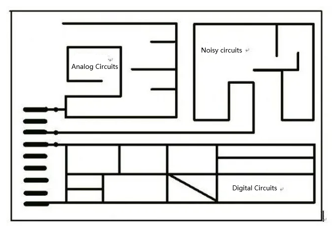
(1) The PCB board is pre-divided into digital, analog and DAA signal wiring areas.
(2) Digital and analog components and corresponding alignments are separated and placed in their respective wiring areas as much as possible.
(3) High-speed digital signals are routed as short as possible.
(4) Sensitive analog signals are routed as short as possible.

(5) Reasonable allocation of power and ground.
(6) DGND, AGND, and field are separated.
(7) Power and critical signal alignment using wide lines.
(8) Power and ground lines should be as radial as possible, as well as signal lines can not appear back to the loop alignment.
(9) Digital circuits are placed near the parallel bus/serial DTE interface, and DAA circuits are placed near the telephone line interface.
(10) Small discrete device alignment shall be symmetrical, the more closely spaced SMT pad leads should be connected from the pad outside, not allowed in the middle of the pad directly connected.

(11) Priority of key signal lines: Power supply, small signal simulation, high-speed signal, clock signal and synchronization signal and other key signals are given priority.
(12) Wiring density priority principle: start wiring from the devices with the most complex connection relationship on the single board. Start wiring from the most densely connected area on the single board.
(13) PCB design should avoid producing sharp corners and right angles, producing unnecessary radiation, while PCB production process performance is also bad.
(14) SMD pads can not have through holes, in order to avoid the loss of solder paste caused by component soldering. Important signal lines are not allowed to pass between the pin feet.
2. High-Frequency PCB Design Techniques
(1) A reasonable choice of PCB layers. With the middle power layer (vcc layer) and ground layer (Gnd layer) can play a shielding role, effectively reduce parasitic inductance and parasitic capacitance, but also greatly shorten the length of the wiring and reduce the cross-talk between signals.

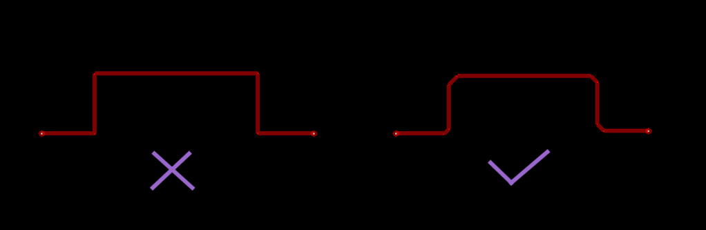
(2) Alignment: must be in accordance with the 45 ° corner way, do not use the 90 ° corner. The following figure.

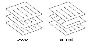
(3) Inter-layer wiring direction: should be perpendicular to each other, the top layer is horizontal, then the bottom layer is vertical, which can reduce the interference between signals.
(4) Wrapped ground: Wrapped ground processing of important signals can significantly improve the anti-interference ability of the signal, but also more interference signals can be wrapped ground, so that it can not interfere with other signals.

(5) Add decoupling capacitor (decoupling capacitor): Add decoupling capacitor to the power supply side of the IC.

(6) High-frequency choke: when there is a digital ground and analog ground and other common ground, to add a high-frequency choke device between them, you can generally use a high-frequency ferrite beads with a central hole through the wire.
(7) Laying copper: increase the area of grounding can also reduce the signal interference. (In the copper laying process need to remove dead copper)

(8) The length of the alignment: the shorter the length of the alignment, the better, in this case, the interference will be reduced. Of course, not all the alignment is only the pursuit of short, such as DDR alignment, is concerned about the clock, address, data alignment between the equal length, so you will see a lot of deliberate efforts to increase the length of the snake alignment.
3.Special components and wires
(1) High-frequency components: the shorter the connection between high-frequency components, the better, try to reduce the distribution parameters of the connection and mutual electrical interference, easy to interfere with the components can not be too close to each other.

(2) Components with high potential difference: the distance between components with high potential difference and connecting lines should be increased to avoid accidental short circuit damage to components. In order to avoid the occurrence of creeping phenomenon, the general requirement of 2000V potential difference between the copper foil line distance should be greater than 2mm.
(3) Weighty components: components with excessive weight should be fixed with brackets.
(4) Heat-generating and heat-sensitive components: Pay attention to the heat-generating components should be far away from the heat-sensitive components. High heat devices should be balanced distribution.
4. Important parameters for PCB wiring design
(1) Copper alignment (Track) line width: single panel 0.3mm, double panel 0.2mm.
(2) Minimum gap between copper foil lines: 0.3mm for single panel, 0.2mm for double panel.
(3) Minimum 1mm from the edge of the PCB board for copper foil lines, minimum 5mm from the edge of the PCB board for components, and minimum 4mm from the edge of the PCB board for pads.
(4) General through-hole mounting components pad diameter is two times the diameter of the inner diameter of the pad.
(5) Electrolytic capacitors should not be close to heat generating components, such as high power resistors, transformers, high power transistors, three-terminal voltage regulators and heat sinks. The distance between electrolytic capacitor and these components is not less than 10mm.
(6) No copper foil wire (except for grounding) and components within 5mm outside the radius of the screw hole.

(7) In a large area of PCB design (more than 500 square meters or more), in order to prevent PCB bending over the tin furnace, should be left in the middle of the PCB a gap of 5mm to 10mm wide not to place the components to be used to prevent PCB bending pressure bar.
(8) Each PCB should be marked with a hollow arrow over the direction of the tin furnace.
(9) Wiring, DIP package IC placement direction should be perpendicular to the direction of the over-tin furnace, try not to parallel, to avoid even tin short circuit.
(10) Wiring direction from vertical to horizontal, should be from 45 ° direction into.
(11) The power line width should not be less than 18mil; the signal line width should not be less than 12mil; the cpu in-out line should not be less than 10mil (or 8mil); the line spacing should not be less than 10mil.
(12) The board wiring should be sparse and dense, when the sparse difference is too large should be filled with mesh copper foil, the grid is greater than 8mil (or 0.2mm).
(13) Drawing wiring area from the edge of the PCB board ≤ 1mm in the area, as well as the installation hole around 1mm, the wiring is prohibited.
(14) PCB with fuses, insurance resistors, AC 220V filter capacitors, transformers and other components in the vicinity of the screen printing layer should be printed on the warning mark.
(15) AC 220V power supply part of the fire wire and zero wire spacing should be not less than 3mm. 220V circuit of any line and low-voltage components and pad, Track between the distance should be not less than 6mm, and screen printed on the high-voltage mark, the weak and strong power should be separated from each other with a thick screen line to warn the maintenance personnel to be careful operation.


