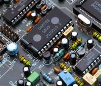
How Your PCBs Are Made Inside the Factory
The PCBs, also known as Printed Circuit Boards, are the physical support of electronic components and the carrier for their electrical interconnection. You’ll find them in many electronic devices like Medical Devices, LEDs, Consumer Electronics, Industrial Equipment, and so on. Depending on their functions in the end products, different types of PCBs are used. They can be Single-sided, Double-sided, Multilayer or Rigid, Flexible and Rigid-flex.
The manufacturing of PCBs is very complicated which involves multiple steps and procedures. In this article, we will have a look at some key steps of the PCB fabrication inside the PCBgogo factory.
1. PCB design and review
The PCB layout is created by the designers using PCB design software such as Altium Designer, OrCAD, Pads, KiCad, Eagle, etc. When the design files are received, the engineer will go over every part of the PCB design to check the potential errors or flaws and make sure the design falls within the manufacturing capabilities of the company. The scope of the checking includes trace widths, trace spacing, hole sizes, and other design parameters. Once the design is approved for production, all the files needed are sent to the factory.

Image courtesy:pcbgogo.com
2. Board cutting
Now it is time to make the actual PCBs. The large-size copper laminates are dry cleaned and cut into smaller pieces suitable for production. During this stage, cleanness does matter as any contaminants or dust would disturb the manufacturing process or affect PCB quality leading to a short or open circuit.
3. Drilling
After cleaning the surface and smoothing the edges, the boards are now ready for drilling. Technically there are three kinds of holes--mechanical holes, through-holes and vias. Mechanical holes are necessary for securing the boards to work stable throughout the manufacturing process. Through-holes aims for putting the leaded components such as resistors, capacitors on the boards while vias serve to establish connections between isolated copper layers.
The drilling machines are computer-guided, using the file from the original design to identify the proper spots to bore. They switch bits automatically--pick up the bit from the drill rack with the correct size, and then load it into the drill bit. An aluminum sheet is also attached to the boards to protect the copper foil from damage during the drilling process.

Image courtesy:pcbgogo.com
4. Electroplating
A good conductivity requires a certain copper thickness on the hole wall which is achieved by electroplating. However, the interior surface of the holes is a non-conductive material such as fiberglass that comprises the interior of the panel. So first, the one micron thick - of copper is deposited over the surface as well as the drilled holes of the panel through the chemical deposition. Electroplating proceeds subsequently to add the required copper thickness to the boards.
To guarantee accuracy, the entire process such as the chemical treatment and cleaning is computer-controlled.

Image courtesy:pcbgogo.com
5. Layer imaging
The next step is to print the design onto the board.
5.1 Exposing
First, the laminate panel is covered by a type of photosensitive dry film with the circuit diagram of the boards. This film is made of photo-reactive chemicals that are hardened after exposure to UV light.
5.2 Developing
Under the powerful UV light, the translucent part of the film is hardened and gets stick to the board while the black areas with the circuit remain unhardened and will be washed off later using an alkaline solution.
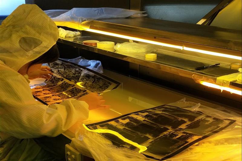
Image courtesy:pcbgogo.com
6. Etching
Then it comes to the next process--etching which removes all the unprotected copper, leaving the desired copper protected by the hardened resists. With all the unwanted resist and copper removed, the circuit diagram is now printed on the board.
7. AOI inspection
After etching, the boards are sent to the automated optical inspection (AOI) where high-resolution cameras automatically scan the PCBs. By comparing the images captured and the original design files, potential defects can be found at the earlier stage. The following features of a PCB are inspected: Line width violations, spacing violation, excess copper, short or open circuits, missing pads, etc... The faculty boards will be reworked while the other boards move to the next process.
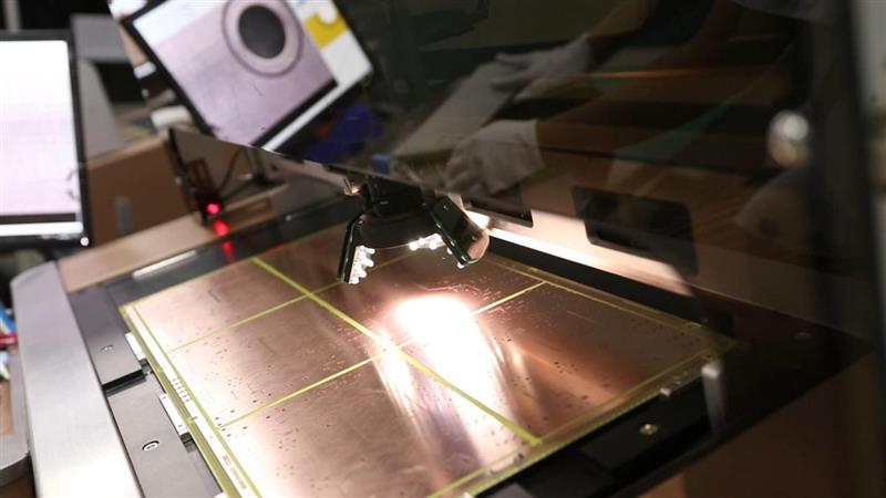
Image courtesy:pcbgogo.com
8. Solder mask
As both sides of the boards are copper layers that are easily oxidized in the air, a solder mask is applied on the surface to prevent the board from external environmental damage. Prior to this process, all the panels are cleaned and covered with an epoxy solder mask ink. Similar to the layer imaging step, the UV light strikes the boards to indicate where the solder mask needs to be removed. The areas uncovered are copper pads for soldering the components.
The solder mask gives PCBs a unique green color. Nowadays, different colors are available according to the design requirement. For example, PCBgogo also offers red, blue, yellow, purple, matte black, and so on.

Image courtesy:pcbgogo.com
9. Silkscreen
Next, the vital information pertaining to the PCBs is printed onto the board, often with an inkjet printer. The information includes pin locators, part numbers, company logo, and so on. Silkscreen printing must be readable and clear to ensure its effectiveness and practicality.
10. Surface finishing
As mentioned in the solder mask step, the exposed copper layers are easy to be oxidized. Thus, the PCBs have their surface finish applied to protect the uncovered copper pads from oxidation that can occur with exposure to air.
The common surface treatment methods are as follows:
-- Hot air solder level (HASL)
-- Organic solderability preservative (OSP)
-- Electroless nickel immersion gold (ENIG)
-- Immersion Tin (ISn)
-- Immersion Silver (IAg)
11. Electrical testing
Going through all the above steps, a PCB is almost finished. Electrical testing is then performed to ensure the functionality of the PCBs and their conformity to the original design. The major types of test equipment are the Flying probe, which is electro-mechanically controlled to test the accessibility problems of the boards.
All the PCBs manufactured in PCBgogo undergo rigorous testing before delivery.
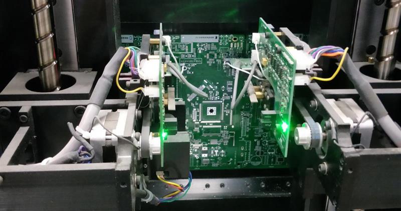
Image courtesy:pcbgogo.com
12.Milling
The last step has now been reached: cutting. Different boards are cut from the original panel to meet the required specifications. Either a router or a v-groove is used in this process. The V-groove creates v-shaped cuts along the sides of the board while a router leaves small tabs along the board edges. Both methods allow the boards to quickly separate without damage.
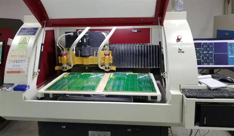
Image courtesy:pcbgogo.com
Conclusion
As presented in this article, PCB manufacturing is a complex process requiring many steps. To guarantee high quality, getting a reliable company to build your PCBs is important. PCBgogo is one of the most experienced PCB and PCB assembly manufacturers in China, processing 4+ factories built in over 2,0000 square meters with the most advanced production equipment. If you are looking for high-quality PCBs with low cost and fast lead time, PCBgogo is definitely your best choice.


