AOI in PCB and SMT Production Line
PCBs are expected to function correctly according to the project specifications. To ensure product quality, PCB manufacturers should institute a variety of inspection techniques during the different production procedures. If the critical errors are identified and fixed at an earlier stage, the cost can be minimized.
The development of surface mounting technology (SMT) and the miniaturization of electronics components brings increasing complexity of PCB design and a geometric increase in the number of solder joints on a board. Some traditional testing techniques such as manual visual inspection can no longer meet the modern quality control requirement. Automated Optical Inspection (AOI), based on the principle of optics and a combination of image acquisition, analysis, computer software, and automatic control technology, is able to detect and process the defects encountered in production in real-time. It is now widely applied in the PCB manufacturing and assembly process.

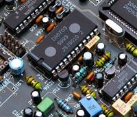
Figure 1 The detected PCB with defects
What is AOI?
The AOI system illuminates the inspected board from various angles and uses high-resolution CCD cameras that automatically scan the board and take images of it. By comparing the images captured with the “golden board” or design specifications, it can evaluate the quality of the bare boards and assembled boards.
Technically, there are two methods used in AOI Technology, Design Rule Checking (DRC) and Image Recognition Technique. As the name suggests, DRC checks the circuits based on the given design requirements. For example, the width of all leads should not be less than 0.127 mm. If the tested board is not within the range, the defects will be highlighted. The Image Recognition Technique is to compare the digital image stored in the AOI system with captured images of the tested boards. The detection accuracy of this method depends on the standard image, the resolution, and the detection program used. As the PCB design rules and standards are constantly being updated, the DRC method based on design rules is not very applicable. Instead, following the rapid development of computer technology and high-speed image processing, the Image Recognition Technique has become the mainstream.
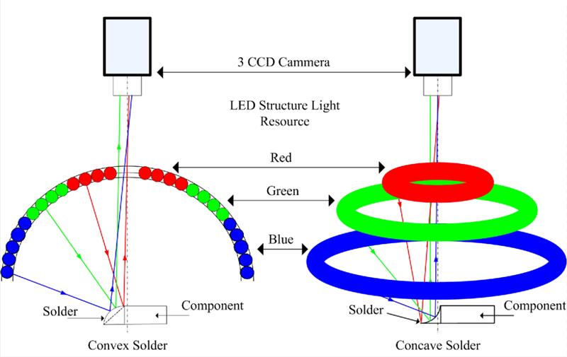
Figure 2 AOI camera system
Application of AOI in PCB and SMT production line
1. In the PCB manufacturing process
The early PCB production has relied on a combination of manual visual inspection and electrical inspection to identify the detects on bare boards. However, they have inherent drawbacks such as low efficiency, low precision and easy to miss detection problems, and so on. As the electronic technology develops, the density and complexity of PCB design increase, these testing methods are no longer a viable option. On the contrary, the significance of AOI becomes apparent.
AOI is mainly applied after the etching process where most of the defects occur. Line width violations, spacing violations, excess copper, short or open circuits, etc... are inspected at this stage. Following this, the defective boards will be reworked while other boards move to the next process. It should be noted that although AOI can find out most of the defects, there are possibilities of missed detection issues or misjudgment as dust, contamination, and poor reflectivity of some materials in the PCB manufacturing process may cause false calls. Therefore, a manual visual inspection should be carried out later if any defects are detected by the AOI system.

Figure 3 AOI inside PCBgogo factory
2. In the SMT assembly process
2.1 After solder paste printing
Solder paste printing is the first step of the SMT process and the root cause of most assembly defects. It is reported that about 30%~70% of the faculty parts of the assembled PCB are directly related to improper solder paste printing. If the defects can be found out and fixed at this stage, the unqualified rate of the final products would be effectively reduced and thus minimize the cost and improve the production efficiency. By detecting the quality of solder paste printing including paste volume & height, paste shape deformities, bridging & displacement, and so on, AOI ensures that the solder paste is correctly deposited on the board.
2.2 Pre-reflow
Once the PCB has been confirmed to have the correct amount of solder paste applied, it moves into the next manufacturing process-- component placement. AOI is capable of checking the component offset, component polarity, component presence or absence, component skew, wrong part, and or other errors that occur at this stage. It is a key step to ensure that all parts have been correctly placed on the board before reflow soldering.
2.3 Post-reflow
Following the component placement process, the boards are directed to the reflow oven machine where the solder paste is heated and the SMD is finally assembled onto the boards. It is important to identify the quality of the solder joint and components. Besides the component offset, component polarity, component presence or absence, component skew, wrong part, AOI at this stage can also identify the defects such as area defects, billboarding, excessive solder joints, flipped component, insufficient paste around leads, insufficient solder joints, lifted leads, tombstoning, and solder bridging. Using AOI at the post-reflow stage is the most popular option for some PCB manufacturers as all assembly errors can be found at this point, which provides a high degree of quality assurance.

Figure 4 AOI inside PCBgogo factory
The future of AOI
AOI is a precise system with accurate positioning and powerful functions. Employing AOI in PCB or SMT production line can conduct a comprehensive inspection of circuits, solder paste printing, component defects, and solder joint defects. It is an essential tool in today’s PCB and SMT industry. So what will be the future development of AOI?
1. Increasing measurement accuracy
The use of any testing techniques in the PCB production line is to find out the defects and minimize false calls. In the future, the measurement accuracy of the newly introduced AOI detection algorithm will be greatly improved, and the misjudgment rate will approach zero. Meanwhile, with the development of camera technology and computer technology, the AOI system will gradually adopt “stereo imaging” and “stereo algorithms” to overcome the limitation of plane detection.
2. More advanced color image processing technology
The future AOI system will make full use of the color information of RGB lighting and capture more accurate color images with 3CCD cameras. By fully extracting different color information of the components, solder joints, and pads, AOI can achieve high efficiency in color image processing and help to identify various defect conditions.
3.3D technology becomes mainstream
Compare to 2D Technology that cannot examine hidden solder joints and measurement of connectors, 3D AOI provides true volumetric height information and enhances the examination coverage. By measuring all 3 dimensions (X, Y, and Height) of the boards, 3D AOI can detect every measurable solder and component defect.
![]()

Figure 5 3D AOI image
Conclusion
The advent of AOI owes to people's pursuit of thinner and lighter electronics products. Although AOI can find out most of the defects, it has limitations such as being unable to inspect hidden or shadowed connections underneath BGAs and other packages. As future electronics towards miniaturization, it is critical to use AOI and other testing techniques in combination to achieve the highest quality standard.
As a leading PCB prototype and PCB assembly services provider, PCBgogo pride itself on its quality control process. They apply leading-edge AOI and other testing machines to ensure that all the boards you receive are of high quality. Contact PCBgogo today for quality PCBs!


