5 aspects that contribute to a reliable PCB
PCB is the core of modern electronics. It is used in all kinds of equipment, from small IoT devices such as wearable devices to servers, medical devices, industrial robots, automobiles, and aircraft. Now no electronic products can be made without a PCB. The PCB provides electrical connection, insulation, and mechanical placement of the electronic components that make up the circuit. No matter in the PCB assembly process or in actual use, PCB should of high reliability so as to perform its intended functions under stated conditions for a specified time. In today’s article, we will discuss 5 key aspects contributing to a reliable PCB.

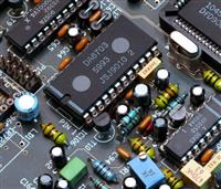
Figure 1:PCBs manufactured by PCBGOGO
Qualified substrate materials
The first consideration in selecting a substrate for your PCB is (soldering and operating) temperature, electrical properties, interconnects (soldering components, connectors), structural strength and circuit density, etc., followed by material and processing costs. After determining which types of substrate to use, special attention should be paid to the quality itself. For example, if the unknown brand FR-4 board with poor mechanical properties is used, the PCB would not perform as expected in the assembled condition. Delamination, open circuit and warpage, and poor impedance performance may also occur. Reliable PCB manufacturers should always use internationally known material for production and be able to provide testing reports for the substrate they use.

Figure 2:Testing reports on PCBGOGO quote page
Specified tolerances for mechanical features and impedance control
Strict controlled mechanical tolerances facilitate the alignment/mating during the assembly process. Some problems such as press-fit pins are only discovered when the assembly is complete. At that time, the rework and modification of PCB will be complex and costly. In addition, if the dimensional deviations of the PCB increase, it might not fit into the final application.
For high-frequency, high-speed PCB where impedance control is a key factor, characteristic impedance(Z0)has to maintain a strict tolerance. If the Z0 deviation exceeds ±10%, it might encounter problems such as Reflection, Dissipation, Attenuation, or Delay during the signal transmission and eventually lead to the failure of the final products. Therefore, the manufacturers should specify a strict tolerance as required.
Adequate copper on the hole walls
A good electrical connection requires a certain copper thickness on the hole wall, usually 25 μm. As the interior surface of the holes is a non-conductive material, the one-micron thick copper is deposited first over the surface and the drilled holes through the chemical deposition. Electroplating proceeds subsequently to add the required copper thickness to the boards. To guarantee accuracy, the entire process is computer-controlled.

Figure 3: Electroplating line inside PCBGOGO factory
A thickness of 25μm copper enhances the reliability of the PCB. Otherwise, it may encounter electrical connectivity issues such as inner layer separation, hole wall fracture during the assembly process, and the possibility of failure under load conditions in actual use.
UL certified solder mask ink
The solder mask is coated on the board and traces where soldering is not needed. It aims to prevent bridging between lines during the assembly process while providing a permanent electrical environment and a protective layer for the PCB that resists chemicals, heat, and insulation. The ink used therefore should be high-quality and safe in order to play its role. Poor quality ink can lead to a detachment between the solder mask and the board and eventually result in corrosion of the copper circuit.
The thickness of the solder mask layer is also an aspect that needs attention. Solder mask of appropriate thickness improves electrical insulation properties, reduces the risk of peeling or loss of adhesion, and increases resistance to mechanical shock. Poor insulation properties due to thin solder masks can cause short circuits when facing unexpected electrical connectivity / arcing.
Rigorous quality testing before delivery
Quality testing is an essential part of the PCB prototype stage as it allows us to identify and correct the defects at an early stage, which helps to reduce cost, save time and optimize safety. The common testing technique includes flying probe test, AOI, AXI, and also IC programming and functional testing as required.
Any quality issue would weaken the performance of the PCB and the final products. To ensure the high reliability of PCB, a combination of testing techniques should be carried out during the different manufacturing processes.

Figure 4: Flying probe testing inside PCBGOGO factory
Conclusion
PCBs look similar on the surface, regardless of their intrinsic quality. It is through the surface and going inside that we can see the differences critical to the durability and functionality of the PCB throughout its life. As the speed and density of electronic devices increase, the importance of the PCB, which is the heart of the device, is further increasing. The miniaturization of components and increasing complexity of PCB design also propose a higher requirement on PCB reliability. Before ordering your PCB prototype, make sure that the PCB manufacturer is qualified with the above factors.


