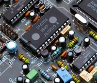
5G PCB
5G PCB
PCBs are the main structure on which electronic components for various devices are built. Aside from making electronic connections possible in electronic devices, PCBs also receive and transmit digital, analog, high-frequency signals. The PCBs for most current devices are built to 4G PCBs. That is, those devices were designed to suit 4G systems. The 4G network has low speed and bandwidth channels when compared to 5G. To be more specific, 4G systems function at frequencies between 600MHz to 5.925Hz - thus below 6 GHz.
But in recent times, the world is gradually advancing towards 5G networks for super-fast signal transmissions. The advent of the 5G network means devices - mobile, telecommunication devices, etc would require high-speed PCBs that suit 5G. This is because the 5G network is required to operate at higher frequency regions of 26 GHz, 30 GHz, and 77 GHz depending on the type of application. This will make the 5G network 10 times faster than the 4G network. The 5G aims to provide 10-20 times higher transmission rates, 100 times higher data capacity, and 10 times higher connection per square kilometer. It is also required to offer 1-millisecond latency.
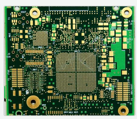
Figure 1. 5G PCB manufactured by pcbgogo.com
Because the 5G network supports higher frequencies and data rates, PCB designers need to employ various ways to design high-frequency 5G PCBs that support 5G. But this comes with challenges. In this article, we will explore some of the design challenges 5G PCBs present and what can be done to overcome them. We will explore some of the best techniques that can be used to design well-functioning 5G PCBs that support the 5G network. You will also get to know some of the key applications of 5G PCB applications. Whether you desire to learn more about 5G PCBs or you want to make a well-informed decision on 5G PCB, this article will be helpful to you. Let's dive in.
5G PCB Design Challenges and Their Solutions
As we mention earlier on, the design of 5G PCB comes with several challenges. Below are some of those challenges and how they can be addressed.
Thermal Management Challenges
As 5G systems operate at higher frequencies, they produce massive heat. Using materials with poor thermal conductivity for 5G PCBs will result in the peeling of copper trace, warping, shrinking, and delamination, which in turn will damage the 5G PCB.
To manage these high temperatures properly, you need to use materials with high thermal conductivity and thermal coefficient. Materials having excellent thermal conductivity and steady dielectric constants will help produce 5G PCBs that can handle the demands of the 5G application.
EMI Shielding
A common challenge of the 5G network needs is EMI, crosstalk, and parasitic capacitance. A sure way to overcome those challenges is to separate the traces on the board. Using a multilayer PCB offers the opportunity to separate high-speed traces so that analog and digital signal routes would be placed far from each other while ensuring DC and DC circuits are kept apart.
To identify and address signal degradation issues and defects on the board, it is imperative to use automated optical inspection (AOI) and 2D metrology to inspect the copper traces and also measure them.
Extremely High-Frequency
Employing extremely high frequency – EHF – in 5G Network presents a major challenge for PCB designers. This is because 5G's millimeter waves move by a line of sight and experience massive attenuation when they come across buildings and unfavorable weather conditions like rain or humidity.
To address this issue, there should be more base stations to provide support to the 5G system. There will be a need for multiple phased array antennas to make beamforming possible. This means mobile devices and base stations would have 5G PCBs incorporated with multiple Antenna Array Units (AAU) together with massive MIMO technology.
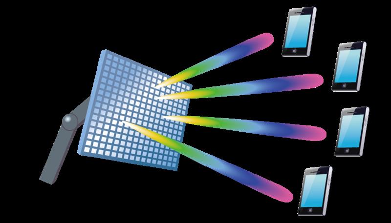
Figure 2. 5G Beamforming
High Bandwidth Per Channel
Another major challenge the 5G network brings in the development of 5G PCB is high bandwidth per channel. For devices and infrastructure that support the 4G network, the bandwidth per channel used is 20 MHz. On the other hand, the 5G network would require 100 MHz frequencies under 6 GHz and 400 MHz beyond 6 GHz. These specifications of the 5G network will require materials having low dielectric transmission loss and higher thermal conductivity. This is primarily because the RF front end will be directly added to the 5G PCB board. For applications operating beyond 6 GHz, you need to use PCB materials that suit the substrate of the mmW frequency band for the 5G PCB.
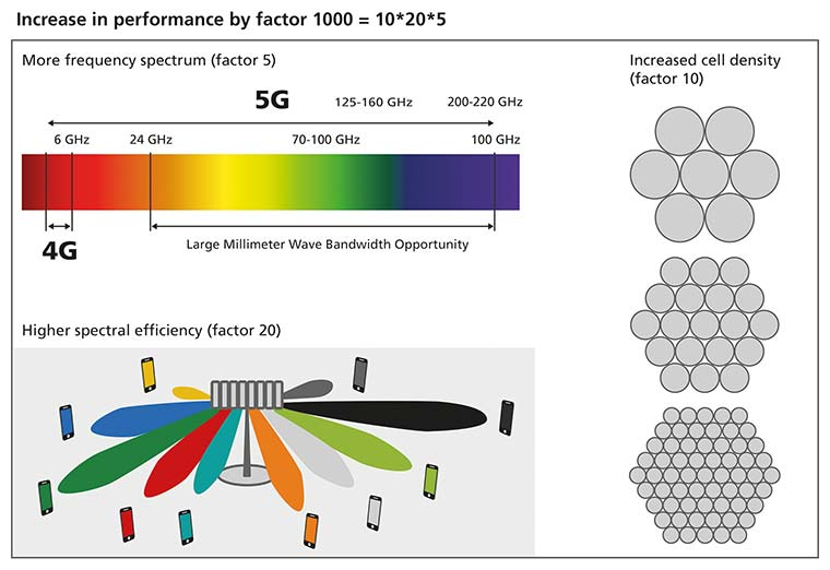
Figure 3 . Features of the 5G and 4G network
Design Considerations for 5G PCBs
The major goal of designers when designing 5G PCBs is to ensure the boards made for various 5G applications would be able to manage mixed high speed and high-frequency signals. Designers should also aim to design 5G boards that offer excellent signal integrity, proper thermal regulation, and excellent impedance control.
Thermal conductivity and thermal coefficient of dielectric constant are the two vital parameters that should be considered when designing 5G PCB.
Below are some major design considerations for efficient 5G PCBs manufacturing:
● Avoid using very thin laminates as this can lead to resonating waves. Thin laminates can also make the wave flow through the conductor.
● 5G PCB designers must prevent EMI which results between components that control analog signals and those that take care of digital signals.
● Use appropriate conductors for transmission lines. Some of the available conductors you can choose from are microstrip, stripline, and grounded coplanar waveguide (GCPW). Those conductors have their advantages and shortfalls. Microstrips are the most popular conductors but they experience radiation losses beyond 30 GHz. Strip lines are good conductors but their manufacturability is difficult. Aside from this, you must connect strip lines to micro vias to the utmost layers. GCPW are excellent but they have higher conduction losses compared to microstrips and strip lines.
● Use high thermal conductivity materials for 5G PCBs because they help to dispel heat produced by the PCB components.
● Use PCB materials with low dielectric constant. Low dielectric constant allows for faster wave speed and up to 30% lower transmission loss.
● Use materials with a thickness between 1/4 and 1/8 of the highest operating frequency’s wavelength.
● Apply a small amount of solder mask on the 5G PCB because it has a high moisture absorption capacity. Using more solder masks will lead to more water absorption which in turn causes high dielectric losses.
● Use smooth copper traces on the board. Using a rough or irregular copper trace will result in an irregular path which will lead to an increase in the resistive losses on the 5G board.
● Employ semi-additive fabrication method to ensure precise trace lines and straight walls on 5G PCB. Semi-additive fabrication has an advantage over traditional fabrication because traditional fabrication often leads to trapezoidal cross-sections, which affects the impedance of the tracks.
● Conduct a robust automatic inspection on the boards to ensure the 5G PCBs are of high quality. This also helps to detect and rectify errors and inefficiencies on the board. Unlike manual inspection, automatic inspection massively saves time and reduces costs during production.
Multilayer 5G PCBs
The specifications of the 5G network require that 5G devices and infrastructure operate at higher frequencies, high temperatures, and high bandwidth per channel. For this reason, 5G devices and infrastructure need multilayer PCBs to help meet those requirements of the 5G network. The 5G PCB is a multilayer PCB that has 3 or more layers stacked together to form a single board. The number of layers of the multilayer 5G PCB depends on its application. Every layer of the multilayer PCB has a circuit component mounted on it.
Multilayer PCBs can accommodate big circuit components because their large number of layers stacked together make them very strong compared to a single layer and double layer PCBs. The unique design and properties of multilayer PCB make them ideal for complex applications like 5G PCB.
Multilayer PCBs have several advantages in the manufacturing of high-frequency boards like the 5G PCB. Below are some of them:
● They allow for an efficient and excellent power distribution on the 5G PCB.
● They supply a great amount of power to 5G devices and other high-frequency board applications
● They allow 5G boards and devices to operate at high speeds and capacity. This is primarily because their multilayered nature allows for more circuit connections.
● They allow for proper heat management on the 5G PCB.
● Multilayer PCB helps to separate high-speed traces on the 5G PCB such that analog and digital signal routes would be positioned far from each other while ensuring DC and DC circuits are kept apart.

Figure 4. 5G PCB
Applications of 5G PCB
5G PCB has several applications across various industries. Below are some popular applications of 5G PCB boards:
High-speed cellular network
The higher speeds at which 5G operates ensure faster communication in services like messaging and calling. With such higher speed, calls and bulk text messaging can be done faster without challenges like unsent messages and call dropping.
Smart Homes
5G PCBs make it possible to connect devices like phones and IPADS to smart devices at homes through a wireless connection to monitor and control activities at home. The super-fast speed of the 5G network helps us to watch live CCTV videos on our mobile phones.
Logistics
Mobile devices made of 5G can be connected to the high-speed 5G network for smooth tracking of logistics on mobile devices. It also makes it possible to properly manage and deliver shipments online on phones.
Entertainment
Thanks to the high speed of the 5G network, you can watch your favorite live shows and movies on Netflix on a 5G PCB-powered mobile device without any breakages. What is more? You can download your favorite videos at an unbeatable speed.
Medical Surgery
High-speed 5G helps to show live videos when doing operations and transplanting on a patient.
Final Thoughts
The world is moving towards the 5G network and this comes with amazing opportunities in the electronic world. But this also presents PCB manufacturers the challenge of manufacturing suitable PCBs that can adopt 5G. In this article, we looked at the massive opportunity 5G offers. We also looked at some of the challenges manufacturers face in 5G PCB design and how they can be addressed to help design compatible and efficient 5G PCBs for various applications. Some of the challenges manufacturers encounter in the design of 5G PCBs are thermal management issues, EMI shielding, extremely high frequency, bandwidth per channel.
By following the recommended design tips outlined in this post, PCB manufacturers can produce well-functioning 5G PCBs that meet the requirements of the 5G network and utilize the massive opportunity offered by 5G. If you need a reliable PCB manufacturer to help you with all your 5G PCB needs, PCBgogo is your best option. PCBgogo offers a quick-turn PCB prototype in as fast as 2-3 days. Express service within 12 hours & 24 hours is also available if your project is urgent. We apply leading-edge machines and procedures to handle all of your PCB prototype requirements at our state-of -art-facility.
With our unmatched PCB experience, expertise, and best-in-class equipment, PCBgogo can help you produce high-quality and efficient PCBs for various applications at a short turnaround time. Contact PCBgogo now for unique and reliable 5G PCBs.


