


4 Layer Mother Board PCB Layout

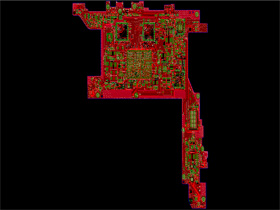
6 Layer Mother Board PCB Layout

6 Layer Mother Board PCB Layout

6 Layer Mother Board PCB Layout
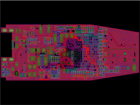
8 Layer AIO Mother PCB Board Layout
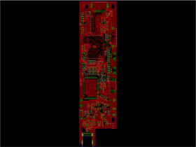
Selfie stick Mother board PCB Layout
TV BOX Mother Board PCB Layout
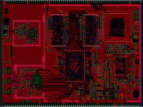
Universal PCB Layout