What is PCB panelization?
What Is PCB Panelization?
PCB layout, which may be the most important aspect of PCB design, it defines the traces and drilling, as well as where the components will be mounted. These specifications and spacing determine whether your layout can be manufactured. Another important layout specification, which is board edge clearance, determining your PCB panelization for manufacturing and assembly. What’s more, it is not only cost-effective, but also can help your PCB manufacturing. Now PCBGOGO will explain what is PCB panelization. And how it can help you with your manufacturing needs.

What is PCB panelization?
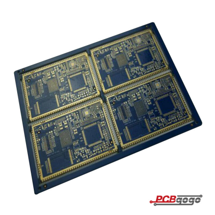
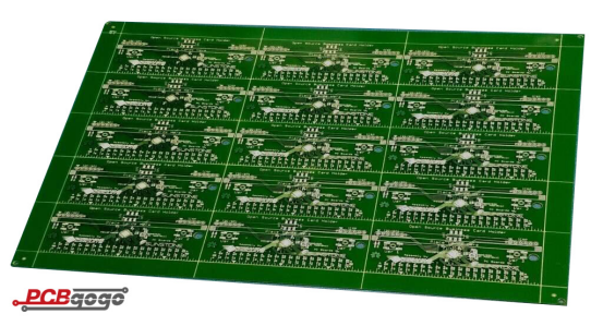
PCB panelization is a fabrication technique, which makes it easy to pass through the assembly line because the smaller PCBs are fabricated and connected together as a single array. And it’s easy for each board to depanelize or remove from the array so that packaging or installing into the product. Alternatively increasing the width to fit on the assembly line with a PCB processing edge around an individual PCB.
There are some factors you need to take into consideration if you want to get the benefits of mass production that come with panelization. The details are as follows:
Component layout: It may limit your panelization options in the placement of components and connectors, where particularly those hanging off the edge of a PCB. So please pay attention to the location of sensitive SMT (surface mount technology) components towards the edge of a PCB.
Tooling holes: there can provide the space for tooling holes on the processing edges of arrays and break-away so that it can do automated testing on the assembly line.
PCB shape: your PCB shape can complicate panelization. Although rectangles are ideal, the alternating images from 90° to 180° can make a great effect on maximizing space on a panel if your PCB shape is complex. And it can fit unusually shaped PCBs into an array with a CAD program.
PCB-array strength: there is a tradeoff between array integrity and the ease of depanelization during production. It can increase strength and reduce vibration with increasing the board count for each array.
The benefits of PCB panelization
It’s necessary to make sure the each board is uniform during the PCB manufacturing process. Some boards may not meet the demands of its intended application without uniformity, so it will be discarded. With the PCBs are more and more smaller, it needs to change the manufacturing processes so that make sure the quality is great. PCB panelization can do well in addressing these problems with keeping smaller boards attached to one another in a larger array.

PCB panelization not only makes a good effect on fitting in standard manufacturing processes for smaller PCBs, but also improving the efficiency when it fabricates your PCBs.
Mass production. The panelization will be cost-effective if you need yo fabricate many PCBs.
Speed and efficiency. It’s more faster and more efficient to process multiple PCBs immediately as part of a large array from paste printing to component assembly, soldering, and even testing.
Product safety. Panelization prevents the boards from shock and vibration experienced during assembly.
Standard panel sizes. It’s more cost-effective to fabricate PCBs with the manufacturer’s standard processing panel.
PCB depanelization process
Depanelization is the removal of the boards from the panel. It needs to do the depanelization process before final assembly and testing. As well as it can be done either with a mechanical or laser routing and each has its benefits. Laser routing is an effective way as it can offer the accurate tolerances. Mechanical routing may save your time and money, however it also creates more debris along the way. Therefore, your PCBs may need additional cleaning after depanelization before they are shipped. It’s important for PCB designers to specify and assembly demands in your design files so that make sure that meet the demands of your orders.
PCB depanelization methods
There are two methods for depanelizing PCBs: scoring and routing, which can put into effect individually or jointly by your CM based on PCB shape and component weights, orientations, locations as well as soldering techniques used.
Routing – this most flexible method is used for odd-shaped boards and it’s made up of using a router bit to create three or five-hole breakaway tabs.
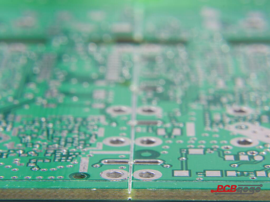
Scoring – it also known as grooves, and it’s made up of cutting a straight-line V-shaped groove into the board ? of the thickness from the top and bottom edge of the panel. Because manual removal can put undue strain on components to the edge, it needs to depanel with a fixture or machine.

Your PCB panelization in PCBGOGO
With over 10 years as an industry leader, PCBGOGO is one of the most experienced PCB and PCB assembly manufacturer in China. highly specialized not only in quick-turn PCB prototype and PCB assembly, but also medium and small volume PCB fabrication. We can provide PCB panelization for you, and we will try our best to meet the demands of panelization as part of your design.
If you have any questions, or need more information on PCB panelization or guidance on creating panels during design, please feel free to contact us with service@pcbgogo.com, we will be happy to help you.

