
What Is Tenting Via And Why It Is Important In PCB Fabrication?
With the development of electronic products and applications of finer pitch devices, vias play an important role in the interconnection between layers in a PCB. Vias are almost in every PCB design, and there are many electronic designers considering them as a fairly simple, straightforward aspect of PCB. There are many PCB manufacturers preferring the tenting method when placing vias. Tenting via is to cover vias with different materials, which allows them to conduct an electrical signal while dissipating any produced heat. Now, let's delve into via tenting and explore why it is important in PCB fabrication.
What is tenting via?
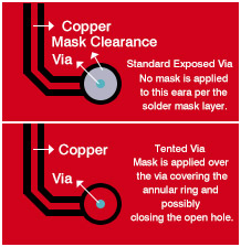
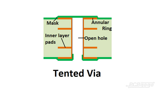
Needless to say, tenting via is the most popular and mature process in PCB fabrication, and tenting vias means to cover the annular ring and via hole with solder mask, which is mainly to cover the annular ring to prevent exposure to the elements and reduce accidental shorting or contact with the circuit. No special steps are taken to ensure the hole opening remains closed. Sometimes, tenting vias will lead to the hole remaining covered, but there is no guarantee, and smaller diameter vias (12mil diameter or less) have the best chance of remaining closed. However, it will have an effect on the PCB fabrication process if there is no solder mask ink in the vias. With the introduction of dry film solder mask, tenting via is easier. Tented vias are useful wherever SMT pads are placed in close proximity to vias. It is particularly useful within BGA areas, where reworking shorts underneath the component is difficult and time-consuming.
Tips: If you make use of the tenting vias in your design, do a fabrication note either in a readme.txt file or a Gerber fab drawing so that we can know you have the intention to remove the mask clearances from some of your vias. Otherwise, we may place the order on an engineering hold to verify your intention.
Related reading: Tening vias, plugged vias, and via in pad
What does it mean to tent a via?
The vias are the holes in your PCB that allow signals to transmit from one side of the board to the other or from one layer of the board to another. In general, the vias are copper-plated as the material is quite conductive. According to the PCB designer, it may expose or cover the holes. So while the manufacturer covers the hole completely, it’s called either a masked or filled via; if the annual ring is merely covered over with the solder mask, it is called tenting the via.
The advantages of via tenting
First of all, provide the solder mask to the vias for protection. It can prevent the copper traces from oxidizing and corroding, just like the solder mask, and the solder mask does the same thing for the via. So, tented via can make an effect on preventing any damage to the PCB layers.
What’s more, it can reduce the number of conductive components that are exposed to external elements with the tenting method. As left exposed, the elements can reduce the integrity of the components and result in corrosion. As well as play a role in reducing the possibility of a short from happening due to solder bridging.
There is no doubt that tenting vias is a cost-effective method; it can provide protection to the vias and the copper around it. And tenting a via with liquid photoimageable solder mask is the most cost-effective method of tenting.
Why is PCB tenting via important?
PCB tenting vias is a common practice to protect printed circuit boards. It is often preferred over mask plugging or epoxy filling due to cost. Tenting a via with liquid photoimageable solder mask is the most cost-effective method of tenting. If you are concerned about the tenting being loose and exposing the annular ring, you can choose the more expensive resin filling.
The main goal of tenting via is to leave fewer conductive pads that are exposed on the surface of the board. Conversely, it means that there are fewer shorts during solder bridging in assembly. What’s more, tenting via also can reduce the paste migration from SMT pads, which will take place while drilling the vias on standard BGA “dog-bone”patterns or while the vias are on the edges of SMT pads. As well as tenting vias can make sure that the via won’t be damaged by exposure to the elements.
In general, tenting is more effective with small vias (diameter of 12 mil or less), so you need to consider closing the via instead with some kind of fill if you have larger vias that you need to protect. Obviously, it will not make an effect on conductivity with filling the vias because electrical travel through the copper plating is unimpeded.
Your PCB fabrication with tenting via in PCBGOGO
With over 10 years as an industry leader, PCBGOGO is one of the most experienced PCB and PCB assembly manufacturers in China. highly specialized not only in quick-turn PCB prototype and PCB assembly, but also in medium and small volume PCB fabrication. Our engineers and production facility are equipped to deal with the intricacy this technique requires with high accuracy. We have used the technology of tenting via for many years, and we know how to ensure a reliable and safe production process.
If you have any questions or need more information on via in pad, please feel free to contact us at service@pcbgogo.com, we will be happy to help you.

